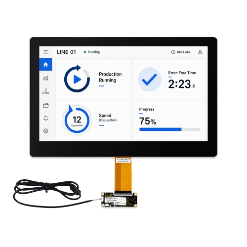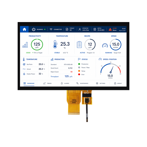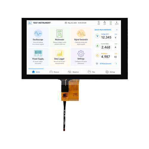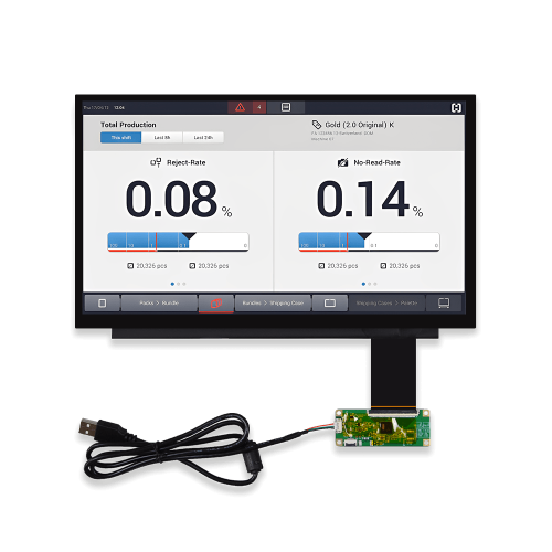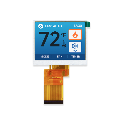
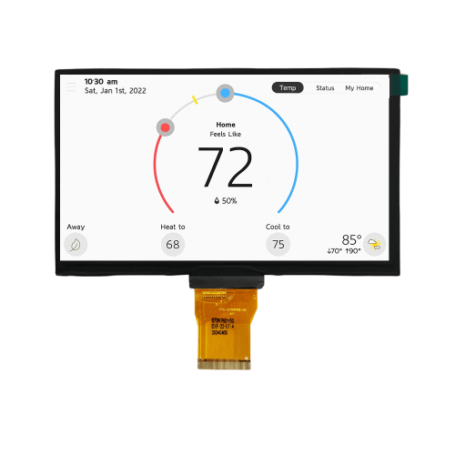
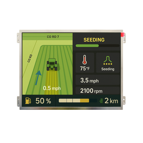
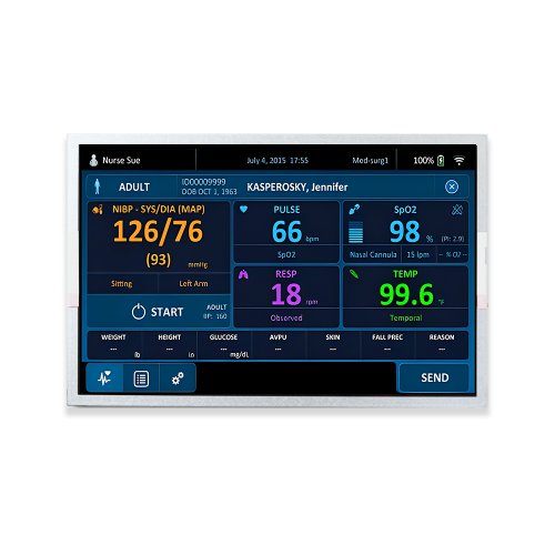





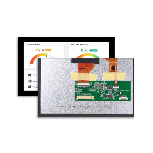
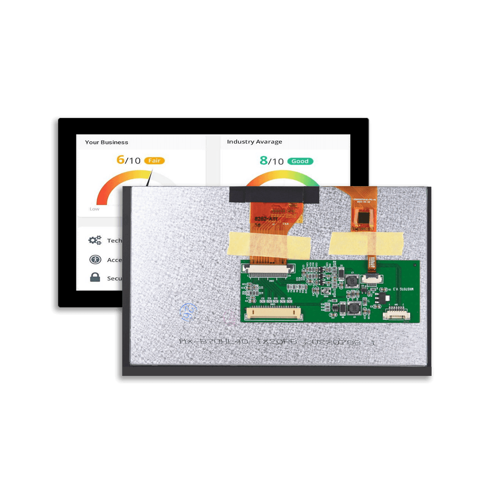
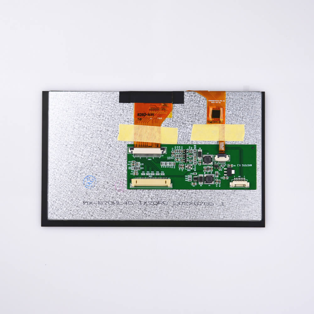
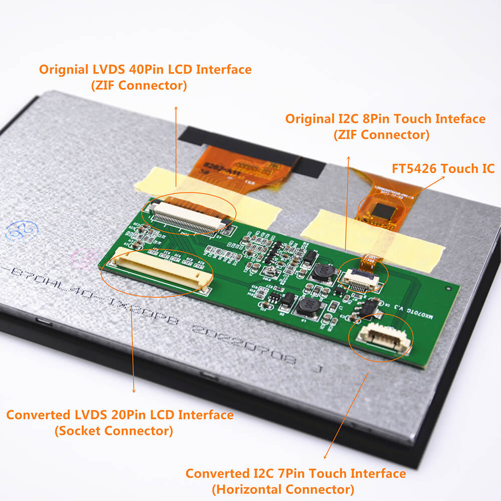
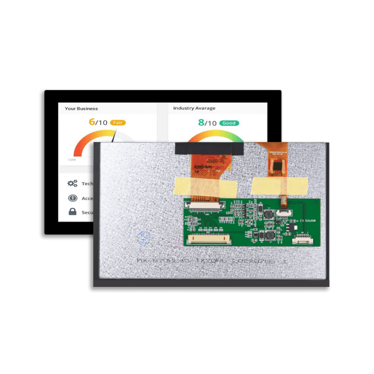
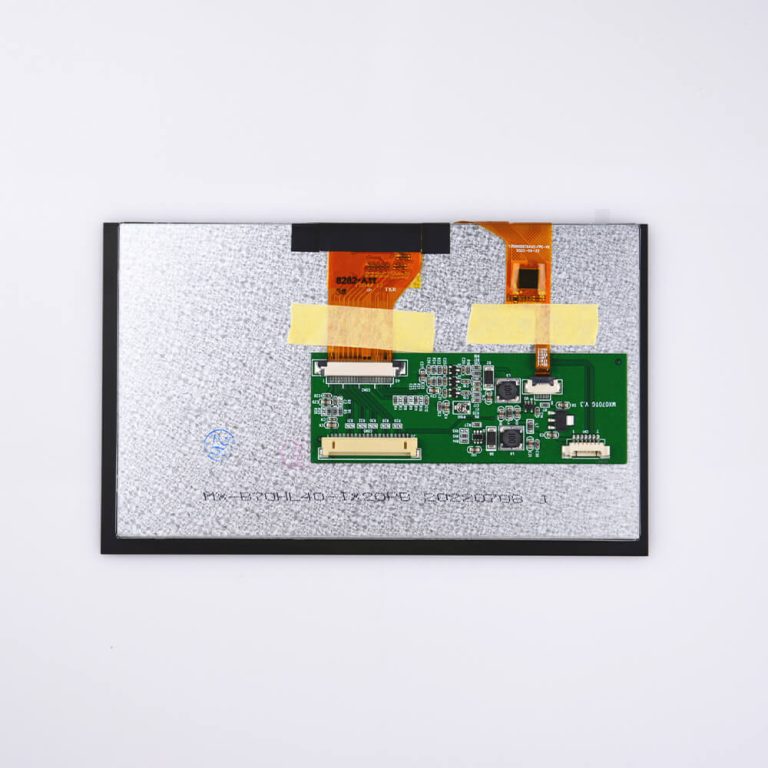

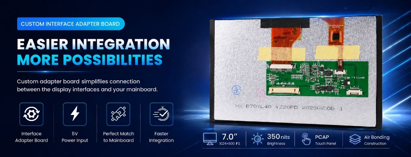
LCM Pin Definition (40-pin LVDS)
| Pin No. | Symbol | Functional |
| 1 | VCOM | Common Voltage |
| 2~3 | VDD | Power Supply for digital circuit |
| 4 | NC | No connection |
| 5 | RESET | Global reset pin |
| 6 | STBYB | Standby mode,Normally pulled high |
| 7 | GND | Ground |
| 8 | Rin0- | -LVDS differential data input |
| 9 | RinO+ | +LVDS differential data input |
| 10 | GND | Ground |
| 11 | Rin1- | -LVDS differential data input |
| 12 | Rin1+ | +LVDS differential data input |
| 13 | GND | Ground |
| 14 | Rin2- | -LVDS differential data input |
| 15 | Rin2+ | +LVDS differential data input |
| 16 | GND | Ground |
| 17 | RclkIN- | -LVDS differential clock input |
| 18 | RclkIN+ | +LVDS differential clock input |
| 19 | GND | Ground |
| 20 | Rin3- | -LVDS differential data input |
| 21 | Rin3+ | +LVDS differential data input |
| 22 | GND | Ground |
| 23-24 | NC | No connection |
| 25 | GND | Ground |
| 26 | NC | No connection |
| 27 | NC | No connection |
| 28 | SELB | 6bot/8bit mode select,L=8 BIT,H=6BIT |
| 29 | AVDD | Power for Analog Circuit |
| 30 | GND | Ground |
| 31-32 | LED- | LED Cathode |
| 33 | L/R | Horizontal inversion |
| 34 | U/D | Vertical inversion |
| 35 | VGL | Gate OFF Voltage |
| 36~37 | NC | No connection |
| 38 | VGH | Gatr ON Voltage |
| 39-40 | LED+ | LED Anode |
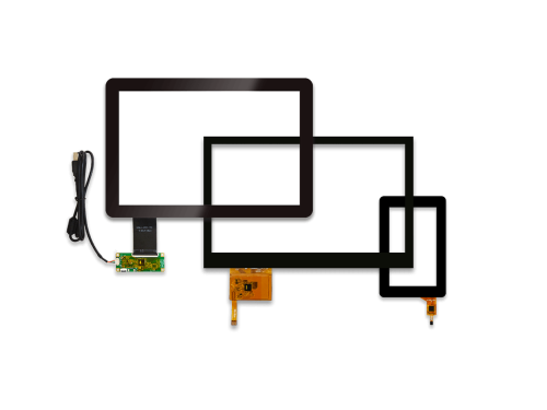
I²C-TP Interface (8-pin I²C)
| PIN | Connection |
| 1 | GND |
| 2 | SCL |
| 3 | SDA |
| 4 | INT |
| 5 | RST |
| 6 | NC |
| 7 | VDD |
| 8 | NC |