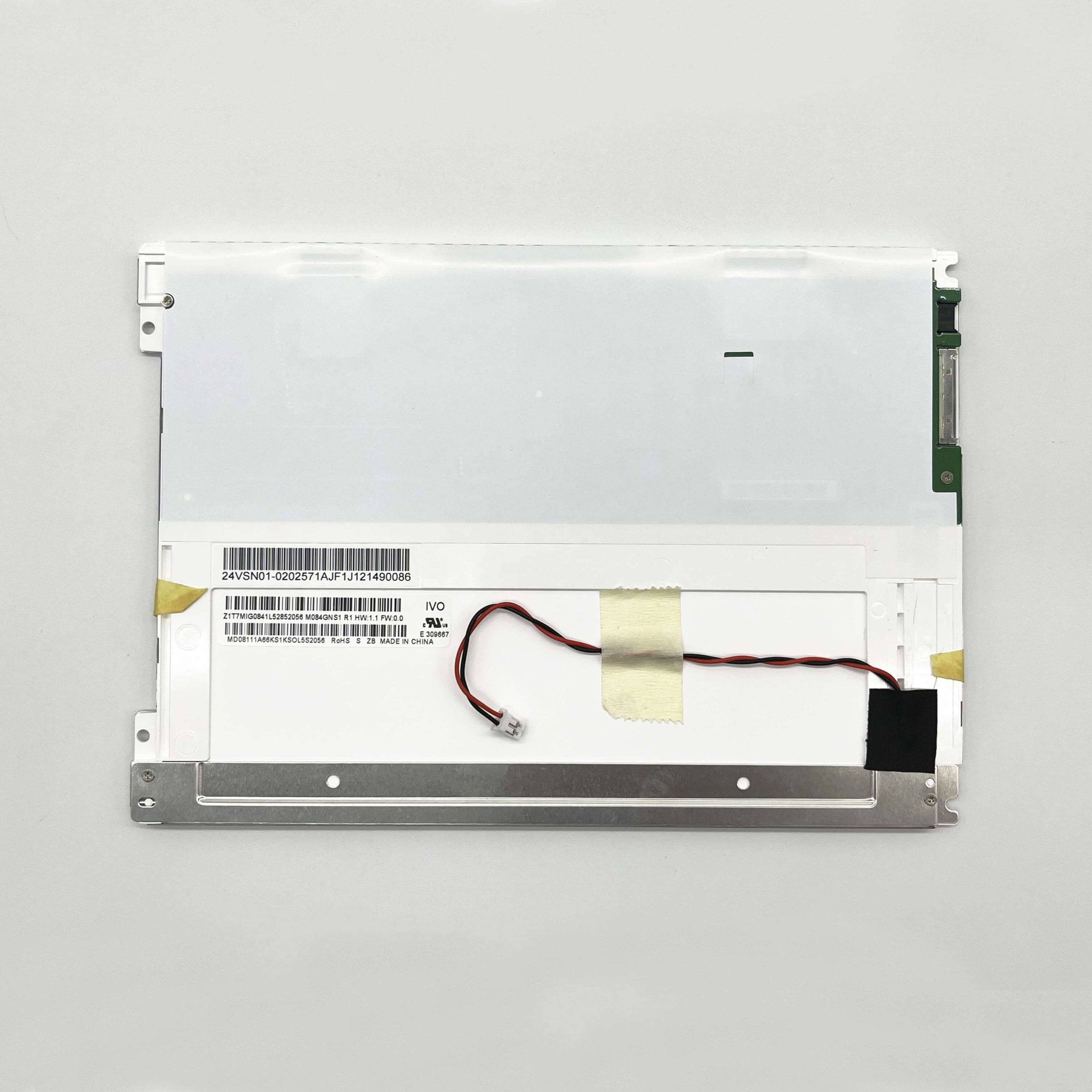
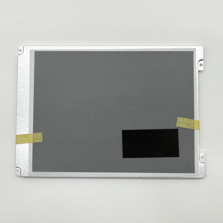

LCM Pin Assignment (20-pin LVDS)
| Pin No. | Symbol | Description |
| 1~2 | VDD | Power Supply 3.3V (typical) |
| 3 | UD | Vertical Reverse Scan control |
| 4 | LR | Horizontal Reverse Scan control |
| 5 | RxIN1- | -LVDS differential data input (R0-R5, G0) |
| 6 | RxIN1+ | +LVDS differential data input (R0-R5, G0) |
| 7 | GND | Ground |
| 8 | RxIN2- | -LVDS differential data input (G1-G5, B0-B1) |
| 9 | RxIN2+ | +LVDS differential data input (G1-G5, B0-B1) |
| 10 | GND | Ground |
| 11 | RxIN3- | -LVDS differential data input (B2-B5, HS, VS, DE) |
| 12 | RxIN3+ | +LVDS differential data input (B2-B5, HS, VS, DE) |
| 13 | GND | Ground |
| 14 | RxCLKIN- | -LVDS differential clock input |
| 15 | RxCLKIN+ | +LVDS differential clock input |
| 16 | GND | Ground |
| 17 | SEL68 | 6/8 bits LVDS data input selection (H:8bit L/NC:6bit) |
| 18 | BIST | H:BIST MODE, L/NC:Normal MODE |
| 19 | RxIN4- | -LVDS differential data input (R6-R7,G6-G7,B6-B7) |
| 20 | RxIN4+ | +LVDS differential data input (R6-R7,G6-G7,B6-B7) |