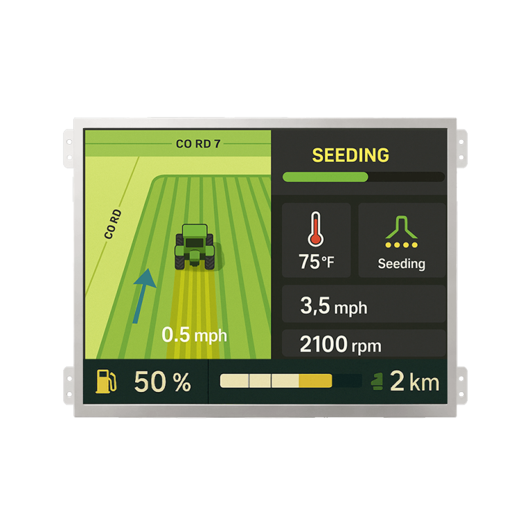
LCM Pin Definition (30-pin LVDS)
| Pin No. | Symbol | Function |
| 1 | NC | Reserved as BIST function for INX test |
| 2 | GND | Ground |
| 3 | Rin3+ | Positive LVDS differential data input (+) |
| 4 | Rin3- | Negative LVDS differential data input (-) |
| 5 | GND | Ground |
| 6 | CLK+ | Clock signal(+) |
| 7 | CLK- | Clock signal(-) |
| 8 | GND | Ground |
| 9 | Rin2+ | Positive LVDS differential data input(+) |
| 10 | Rin2- | Negative LVDS differential data input (-) |
| 11 | GND | Ground |
| 12 | Rin1+ | Positive LVDS differential data input(+) |
| 13 | Rin1- | Negative LVDS differential data input (-) |
| 14 | GND | Ground |
| 15 | RinO+ | Positive LVDS differential data input(+) |
| 16 | Rin0- | Negative LVDS differential data input (-) |
| 17 | GND | Ground |
| 18 | NC | No Connection |
| 19 | GND | Ground |
| 20 | SEL6/8 | Selection for 6 bits/8bit LVDS data input Low or NC: 8 bit input mode High: 6 bit input mode |
| 21 | NC | Reversed as EE_WP for OTP function |
| 22 | NC | Reversed as EE_SDA for OTP function |
| 23 | NC | Reversed as EE_SCL for OTP function |
| 24 | Reverse | Reverse panel function(Display rotation) |
| 25 | GND | Ground |
| 26 | GND | Ground |
| 27 | GND | Ground |
| 28 | VDD | Power supply: +3.3V |
| 29 | VDD | Power supply: +3.3V |
| 30 | VDD | Power supply: +3.3V |
Absolute Maximum Ratings
| Item | Symbol | Min. | Max. | Unit |
| Power Supply Voltage | VDD | -0.3 | 3.6 | V |
| LED_VCCS | -0.3 | 25 | V | |
| Storage Temperature | Tstg | -30 | +80 | ℃ |
| Operating Temperature | Topr | -30 | +80 | ℃ |
LED Backlight Characteristics
| Item | Symbol | Min. | Typ. | Max. | Unit |
| Voltage for LED Backlight | LED+ | 31 | 33 | 35 | V |
| Current for LED Backlight | LED1-/LED2- | 78 | 80 | 82 | mA |