LCM Pin Definition (51-pin LVDS)
| Pin NO. | Symbol | Description | Pin NO. | Symbol | Description |
| 1 | NC(Reverse) | No Connection or Ground | 27 | Bit Select | H'or Open =10bit(D), 'L' =8bit |
| 2 | NC(MPLUS_ON) | No Connection | 28 | R2AN | SECOND LVDS Receiver Signal (A-) |
| 3 | NC | No Connection | 29 | R2AP | SECOND LVDS Receiver Signal (A+) |
| 4 | NC | No Connection | 30 | R2BN | SECOND LVDS Receiver Signal(B-) |
| 5 | NC | No Connection | 31 | R2BP | SECOND LVDS Receiver Signal(B+) |
| 6 | NC | No Connection | 32 | R2CN | SECOND LVDS Receiver Signal (C-) |
| 7 | LVDS Select | 'H'=JEIDA,'L'or Open =VESA | 33 | R2CP | SECOND LVDS Receiver Signal(C+) |
| 8 | NC | No Connection | 34 | GND | Ground |
| 9 | NC | No Connection | 35 | R2CLKN | SECOND LVDS Receiver Clock Signal(-) |
| 10 | NC | No Connection or Ground | 36 | R2CLKP | SECOND LVDS Receiver Clock Signal(+) |
| 11 | GND | Ground | 37 | GND | Ground |
| 12 | R1AN | FIRSTLVDS Receiver Signal (A-) | 38 | R2DN | SECOND LVDS Receiver Signal(D-) |
| 13 | R1AP | FIRST LVDS Receiver Signal (A+) | 39 | R2DP | SECOND LVDS Receiver Signal(D+) |
| 14 | R1BN | FIRST LVDS Receiver Signal(B-) | 40 | R2EN | SECOND LVDS Receiver Signal(E-) |
| 15 | R1BP | FIRST LVDS Receiver Signal(B+) | 41 | R2EP | SECOND LVDS Receiver Signal(E+) |
| 16 | R1CN | FIRST LVDS Receiver Signal (C-) | 42 | GND | Ground |
| 17 | R1CP | FIRST LVDS Receiver Signal(C+) | 43 | GND | Ground |
| 18 | GND | Ground | 44 | AGP or NSB | 'H'or Open=AGP, 'L'=NSB(No signal Black) |
| 19 | R1CLKN | FIRST LVDS Receiver Clock Signal(-) | 45 | GND | Ground |
| 20 | R1CLKP | FIRST LVDS Receiver Clock Signal(+) | 46 | GND | Ground |
| 21 | GND | Ground | 47 | NC | No connection |
| 22 | R1DN | FIRST LVDS Receiver Signal (D-) | 48 | VLCD | Power Supply+12.0V |
| 23 | R1DP | FIRST LVDS Receiver Signal(D+) | 49 | VLCD | Power Supply+12.0V |
| 24 | R1EN | FIRST LVDS Receiver Signal (E-) | 50 | VLCD | Power Supply +12.0V |
| 25 | R1EP | FIRST LVDS Receiver Signal(E+) | 51 | VLCD | Power Supply+12.0V |
| 26 | GND | Ground | - |
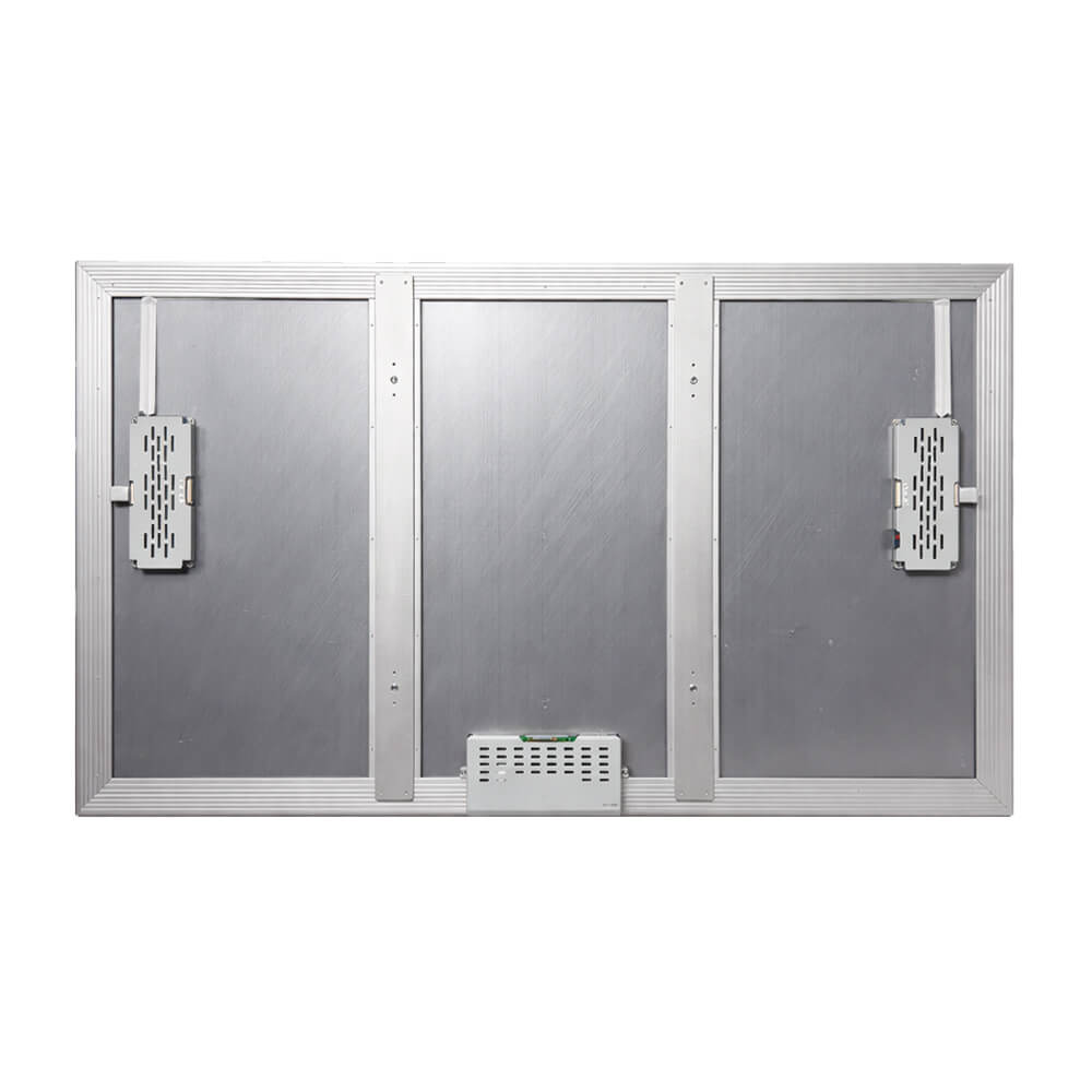
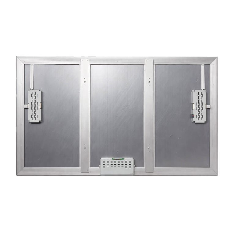
Backlight Interface Connection
CN2: Input terminal
| PIN# | Symbol | Description | ||
| 1 | VDDB | Operating Voltage Supply,+24V DC Regulated | ||
| 2 | VDDB | Operating Voltage Supply,+24V DC Regulated | ||
| 3 | VDDB | Operating Voltage Supply,+24V DC Regulated | ||
| 4 | VDDB | Operating Voltage Supply,+24V DC Regulated | ||
| 5 | VDDB | Operating Voltage Supply,+24V DC Regulated | ||
| 6 | GND | Ground | ||
| 7 | GND | Ground | ||
| 8 | GND | Ground | ||
| 9 | GND | Ground | ||
| 10 | GND | Ground | ||
| 11 | NC | Not connect | ||
| 12 | VBLON | BL On-Off: High (2.5~5.5V) for BL, Low/Open(0~0.5V) for BL off | ||
| 13 | PDIM(note 1) | DC Dimming High (5.0V/100%Duty) for 100%Lum. |
||
| 14 | PDIM | PWM Dimming High (OV/100%Duty) for 100%Lum. |
||
CN3: Input terminal
| PIN# | Symbol | Description | |
| 1 | VDDB | Operating Voltage Supply,+24V DC Regulated | |
| 2 | VDDB | Operating Voltage Supply,+24V DC Regulated | |
| 3 | VDDB | Operating Voltage Supply,+24V DC Regulated | |
| 4 | VDDB | Operating Voltage Supply,+24V DC Regulated | |
| 5 | VDDB | Operating Voltage Supply,+24V DC Regulated | |
| 6~10 | GND | Ground | |
| 11~14 | NC | No Connect | |
Absolute Maximum Ratings
| Parameter | Symbol | Value | Unit | ||
| Min | Max | ||||
| Power Input Voltage | LCD Circuit | VLCD | -0.3 | +14.0 | VDC |
| T-Con Option Selection Voltage | VLOGIC | -0.3 | +4.0 | VDC | |
| Operating Temperature | ToP | 0 | +50 | ℃ | |
| Storage Temperature(without packing) | TST | -20 | +60 | ℃ | |
| Panel Front Temperature | TSUR | - | +68 | ℃ | |
| Operating Ambient Humidity | HoP | 10 | 90 | %RH | |
| Storage Humidity | HST | 5 | 90 | %RH | |
Electrical Characteristics
| Parameter | Symbol | Value | Unit | |||
| Min | Typ | Max | ||||
| Circuit: | ||||||
| Power Input Voltage | VLCD | 10.8 | 12.0 | 14 | VDC | |
| Power Input Current | ILCD | - | 453 | 588 | mA | |
| - | 578 | 751 | mA | |||
| T-CON Option Selection Voltage | Input High Voltage | VIH | 2.7 | - | 3.6 | VDC |
| Input Low Voltage | VIL | 0 | - | 0.7 | VDC | |
| Power Consumption | PLCD | - | 5.4 | 7.1 | Watt | |
| Rush current | IRUSH | - | - | 8 | A | |
LED Backlight Characteristics
| Item | Symbol | Condition | Min | Typ | Max | Unit | |
| Power Supply Input Voltage | VDDB | - | 22.8 | 24 | 25.2 | V | |
| Power Supply Input Current | lDDB | VDDB=24V | - | 9.58 | - | A | |
| Power Consumption | PDDB | VDDB=24V | - | 230 | - | Watt | |
| Inrush Current | lRUSH | VDDB=24V | - | - | TBD | A | |
| Control signal voltage | Vsignal | Hi | VDDB=24V | 2.5 | 5.5 | V | |
| Low | 0 | - | 0.8 | ||||
| Control signal current | lsignal | VDDB=24V | - | - | 1.5 | mA | |
| External PWM Duty ratio (input duty ratio) |
D_EPWM | VDDB=24V | 0 | - | 100 | % | |
| External PWM Frequency |
F_EPWM | VDDB=24V | 100 | - | 1000 | Hz | |
| External DC Duty ratio (input duty ratio) |
D_E DC | VDDB=24V | 25 | - | 100 | % | |
| External DC Voltage |
V_E DC | VDDB=24V | 0 | - | 5.0 | V | |
| External induction dimming | (Duty ratio) | VDDB=24V | 25 | - | 100 | % | |
| Input Impedance | Rin | VDDB=24V | TBD | - | - | Kohm | |
| LED lifetime | LTLED | - | - | 50,000 | - | Hr | |