


| Pin No. | Symbol | Function | Remark |
| 1 | RXO0- | Negative Transmission data of Pixel 0 (ODD) | |
| 2 | RXO0+ | Positive Transmission data of Pixel 0 (ODD) | |
| 3 | RXO1- | Negative Transmission data of Pixel 1 (ODD) | |
| 4 | RXO1+ | Positive Transmission data of Pixel 1 (ODD) | |
| 5 | RXO2- | Negative Transmission data of Pixel 2 (ODD) | |
| 6 | RXO2+ | Positive Transmission data of Pixel 2 (ODD) | |
| 7 | BIST | Bistfunction | Bist function |
| 8 | RXOC- | Negative Transmission Clock (ODD) | |
| 9 | RXOC+ | Positive Transmission Clock (ODD) | |
| 10 | RXO3- | Negative Transmission data of Pixel 3 (ODD) | |
| 11 | RXO3+ | Positive Transmission data of Pixel 3 (ODD) | |
| 12 | RXE0- | Negative Transmission data of Pixel 0 (EVEN) | |
| 13 | RXE0+ | Positive Transmission data of Pixel 0 (EVEN) | |
| 14 | GND | Power Ground | |
| 15 | RXE1- | Negative Transmission data of Pixel 1 (EVEN) | |
| 16 | RXE1+ | Positive Transmission data of Pixel 1 (EVEN) | |
| 17 | GNG | Power Ground | |
| 18 | RXE2- | Negative Transmission data of Pixel 2 (EVEN) | |
| 19 | RXE2+ | Positive Transmission data of Pixel 2 (EVEN) | |
| 20 | RXEC- | Negative Transmission Clock (EVEN) | |
| 21 | RXEC+ | Positive Transmission Clock (EVEN) | |
| 22 | RXE3- | Negative Transmission data of Pixel 3 (EVEN) | |
| 23 | RXE3+ | Positive Transmission data of Pixel 3 (EVEN) | |
| 24 | GND | Power Ground | Note 1 |
| 25 | SCL | Internal Use | P-Gamma |
| 26 | SDA | Internal Use | P-Gamma |
| 27 | NC | Not Connection | |
| 28 | VDD | Power Supply: +5V | |
| 29 | VDD | ||
| 30 | VDD |
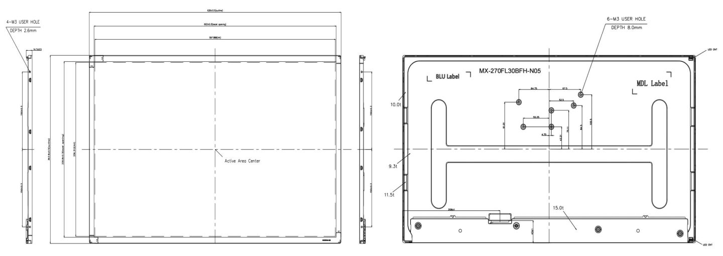
Note 1 : This pin should be connected with GND.
| Pin No. | Description |
| 1 | LED current sense for string 1 |
| 2 | LED current sense for string 2 |
| 3 | LED power supply |
| 4 | LED power supply |
| 5 | LED current sense for string 3 |
| 6 | LED current sense for string 4 |
| CONNECTOR | CI1406M1VL0-NH |
| Parameter | Symbol | Min. | Max. | Unit | Remark |
| Power Supply Voltage |
VDD |
VSS-0.3 | 6 | V | Ta=25℃ |
| Operating Temperature |
TOP |
0 | +60 | ℃ | Note 1 |
|
TSUR |
-20 | +80 | ℃ | ||
| Storage Temperature |
TST |
-30 | +80 | ℃ | |
| Operating Ambient Humidity |
HOP |
10 | 80 | %RH | |
| Storage Humidity |
HST |
— | 90 | %RH |
Note 1: Temperature and relative humidity range are shown in the figure below.
Wet bulb temperature should be 39C max. and no condensation of water.
| Parameter | Min. | Typ. | Max. | Unit | Remarks | |
| Power Supply Voltage |
VDD |
4.5 | 5.0 | 5.5 | V | Note l |
| Permissible Input Ripple Voltage |
VRF |
— | — | 300 | mV | Note 1,3 |
| High Level Differential Input Threshold Voltage |
VIH |
— | — | +100 | mV | — |
| Low Level Differential Input Threshold Voltage |
VIL |
-100 | — | — | mV | |
| Differential Input Voltage | |VID| | 200 | — | 600 | mV | — |
| Differential Input Common Mode Voltage |
Vcm |
1.0 | 1.2 | 1.5 | V | VIH=100mV, VIL=-100mV |
| Power Consumption |
PD |
— | 6.5 | 8.8 | W | @60/75HZ |
|
PBL |
— | 63.5 | 67.7 | W | Note 4 | |
|
Ptotal |
— | 37 | 41.2 | W | — | |
Notes:
1. The supply voltage is measured and specified at the interface connector of LCM. The current draw and power consumption specified is for VDD=5.0V, Frame rate=75Hz, Clock frequency=92.9MHz.
2. Duration of rush current is about 2ms and rising time of VDD is 520μs±20%.
3. Ripple Voltage should be covered by Input voltage Spec.
4. Calculated value for reference (Input pins*VPIN ×IPIN) excluding inverter loss.
| Parameter | Min. | Typ. | Max. | Unit | Remark | |
| LED Light Bar Input Voltage Per Input Pin |
VPIN |
— | 69 | 73.6 | V | Duty 100% |
| LED Light Bar Input Current Per Input Pin |
IPIN |
— | 115 | — | mA | Note 1,2 |
| LED Power Consumption |
PBL |
- | 63.5 | 67.7 | W | Note 3 |
| LED Life-Time | — | 50,000 | — | — | Hrs | Note 4 |
LED bar consists of 92 LED packages, 4 strings (parallel) × 23 packages (serial).
Note 1: There are two light bars, and the specified current is the input LED chip 100% duty current.
Note 2: The sense current of each input pin is 115 mA.
Note 3: PBL=8 input pins × VPIN × IPIN.
Note 4: The lifetime is defined as the time at which the luminance of the LED becomes 50% of the initial brightness, or abnormal lighting occurs, at IPIN=115 mA under continuous operation at 25 ± 2 ℃.