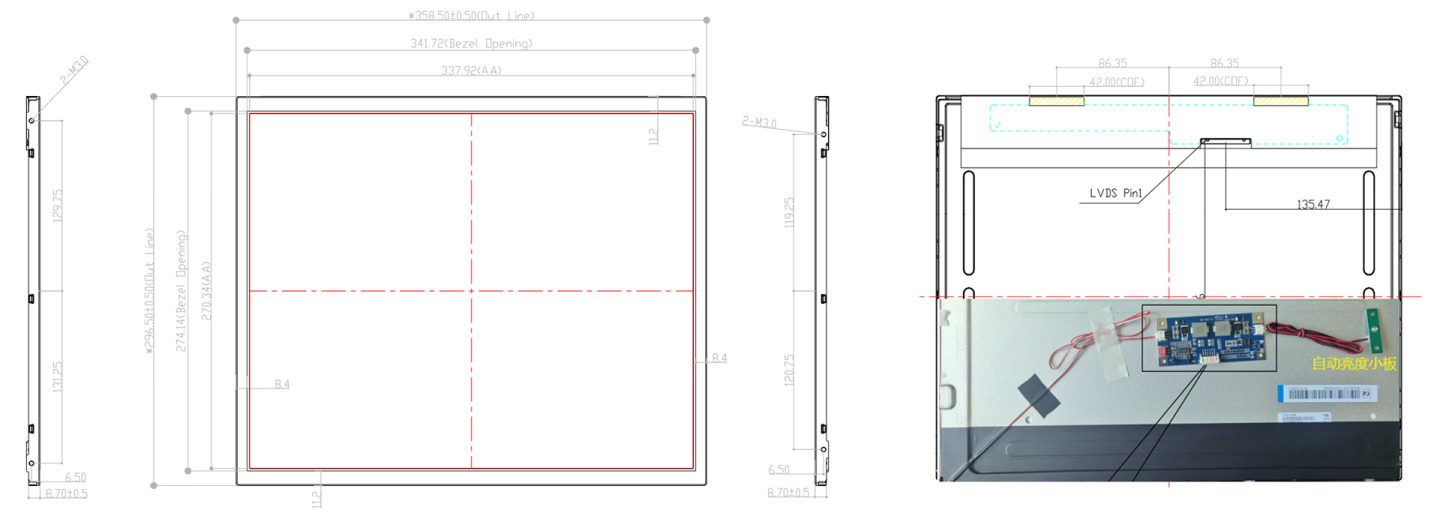


| Pin No. | Symbol | Description | Pin No. | Symbol | Description |
| 1 | RXO0- | Negative LVDS differential data input(Odd data) | 16 | RXE1+ | Positive LVDS differential data input(Even data) |
| 2 | RXO0+ | Positive LVDS differential data input(Odd data) | 17 | GND | Ground |
| 3 | RXO1- | Negative LVDS differential data input(Odd data) | 18 | RXE2- | Negative LVDS differential data input(Even data) |
| 4 | RXO1+ | Positive LVDS differential data input(Odd data) | 19 | RXE2+ | Positive LVDS differential data input(Even data) |
| 5 | RXO2- | Negative LVDS differential data input(Odd data) | 20 | RXEC- | Negative LVDS differential data input(Even clock) |
| 6 | RXO2+ | Positive LVDS differential data input(Odd data) | 21 | RXEC+ | Positive LVDS differential data input(Even clock) |
| 7 | GND | Ground | 22 | RXE3- | Negative LVDS differential data input(Even data) |
| 8 | RXOC- | Negative LVDS differential data input(Odd clock) | 23 | RXE3+ | Positive LVDS differential data input(Even data) |
| 9 | RXOC+ | Positive LVDS differential data input(Odd clock) | 24 | GND | Ground |
| 10 | RXO3- | Negative LVDS differential data input(Odd data) | 25 | NC | No connection (for MAXEN internal use) |
| 11 | RXO3+ | Positive LVDS differential data input(Odd data) | 26 | NC | No connection (for MAXEN internal use) |
| 12 | RXE0- | Negative LVDS differential data input(Even data) | 27 | NC | No connection (for MAXEN internal use) |
| 13 | RXE0+ | Positive LVDS differential data input(Even data) | 28 | VDD | Power Supply:+5V |
| 14 | GND | Ground | 29 | VDD | |
| 15 | RXE1- | Negative LVDS differential data input(Even data) | 30 | VDD |
| Pin No. | Symbol | Description |
| 1 | VCC | Power supply voltage +12V |
| 2 | VCC | Power supply voltage +12V |
| 3 | ON/OFF | Output enable signal |
| 4 | DIM | Dimming signal |
| 5 | GND | Power ground |
| 6 | GND | Power ground |
PH2.0-6 (2.0mmX6)
| Parameter | Symbol | Min. | Max. | Unit | Remark |
| Power Supply Voltage |
VDD |
-0.3 | 5.5 | V | Ta=25℃ |
| Operating Temperature |
TOP |
0 | +50 | ℃ | Note 1 |
| Storage Temperature |
TSUR |
-20 | +60 | ℃ | |
|
TST |
-20 | +60 | ℃ | ||
| Operating Ambient Humidity |
HOP |
10 | 80 | %RH | |
| Storage Humidity |
HST |
10 | 80 | %RH |
Note 1: Temperature and relative humidity range are shown in the figure below.
Wet bulb temperature should be 39 ℃ max and no condensation of water.
| Parameter | Symbol | Values | Unit | Remark | |||
| Min | Typ | Max | |||||
| Power Supply Input Voltage |
VDD |
4.5 | 5 | 5.5 | V | Note 1 | |
| Power Supply Current |
IDD |
— | 600 | 1000 | mA | ||
| Power Supply Ripple Voltage |
VRP |
— | — | 300 | mV | — | |
| Rush Current |
IRUSH |
— | 2 | 3 | A | Note 2 | |
| LVDS Interface | Differential Input High Threshold Voltage |
VLVTH |
— | — | +100 | mV | VLVC=12V |
| Differential Input Low Threshold Voltage |
VLVTL |
-100 | — | — | mV | ||
| Common Input Voltage |
VLVC |
0.7 | — | 1.6 | V | — | |
| CMOS Interface | Input High Threshold Voltage |
VIH |
0.7VDD | — | VDD | V | — |
| Input Low Threshold Voltage |
VIL |
0 | — | 0.3VDD | V | — | |
| Power Consumption |
PD |
— | 3 | 5.5 | W | — | |
|
PBL |
— | 26 | — | W | Note 3 | ||
Note 1: The supply voltage is measured and specified at the interface connector of LCM.
The current draw and power consumption specified is for VDD=5.0V, Frame rate fV=60Hz and Clock frequency=54MHz.
Note 2: The duration of rush current is about 2ms and rising time of Power Input is 1ms (min).
Note 3: Reference value = Σ (Vpin × Ipin) for all input pins; inverter loss excluded.