
| Pin No. | Symbol | Description | |||||
| 1 | LEDK | Cathode of LED backlight. | |||||
| 2 | LEDA | Anode of LED backlight. | |||||
| 3 | LED_PWM | Output pad for PWM output signal to driving LED | |||||
| 4 | LED EN | Output pad for enabling LED. | |||||
| S | GND | Power ground. | |||||
| 6 | VDD | Power supply for Analog, Digital System and Booster Circuit. | |||||
| 7 | VDDIO | Power Supply for I/O System. | |||||
| 8 | GND | Power ground. | |||||
| 9 | SCK(DCX) | Clock signal. | |||||
| 10 | MOSI(SDA) | When IM3:Low, SPI interface input/output pin. When IM3:High, SPI interface input pin. The data is latched on the rising edge of the SCL signal. If not used, please fix this pin at VDDI or DGND level. |
|||||
| 11 | MISO(SDO) | SPI interface output pin. The data is output on the falling edge of the SCL signal. If not used, let this pin open. |
|||||
| 12 | D/C(WRX) | Data is regarded as a command when WRX is low. Data is regarded as a parameter or data when WRX is high. |
|||||
| 13 | CS(CSX) | Chip selection signal. | |||||
| 14 | GND | Power ground. | |||||
| 15 | RST | Reset pin, Signal is active low. | |||||
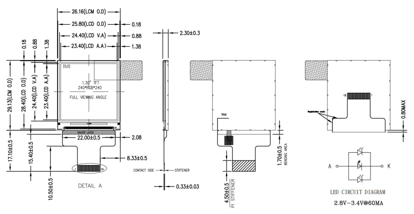
| 16 | IM3 | The MCU interface mode select | |||||
| IM3 | IM2 | IM1 | IM0 | MCU Interface Mode | Data pin | ||
| 0 | 1 | 1 | 0 | 4-line 8-bit serial I/F | SDA: in/out | ||
| 1 | 1 | 1 | 0 | 4-line 8-bit serial I/F Ⅱ | SDA: in/SDO: out | ||
| 17 | TE | Tearing effect signal is used to synchronize MCU to frame memory writing. | |||||
| 18 | GND | Power ground. | |||||
| Parameter | Symbol |
Min | Max | Unit |
| Supply voltage for analog | VDD | -0.3 | 4.6 | V |
| Supply voltage for logic | VDDIO | -0.3 | 4.6 | V |
| Supply current (One LED) | ILED | — | 30 | mA |
| Operating temperature | Top | -20 | +70 | ℃ |
| Storage temperature | Tst | -30 | +80 | ℃ |
Note: The absolute maximum rating values of this product are not allowed to be exceeded at any times. Should a module be used with any of the absolute maximum ratings exceeded, the characteristics of the module may not be recovered, or in an extreme case, the module may be permanently destroyed.
| Item | Symbol | Min | Typ. | Max | Unit |
| Supply Voltage for Analog | VDD | 2.4 | 2.75 | 3.3 | V |
| Supply Voltage for Logic | VDDIO | 1.65 | 1.8 | 3.3 | V |
| Input Voltage | VIL | GND | — | 0.3VDDI | V |
| VIH | 0.7VDDI | — | VDDI | ||
| Input leakage Current | ILKG | -1 | — | 1 | μA |
| Item | Symbol | Value | Unit | Remark | ||
| Min. | Typ. | Max. | ||||
| Voltage for LED Backlight | VF | 2.8 | 3.2 | 3.4 | V | IL=60mA |
| Current for LED Backlight | IL | — | 60 | — | mA | — |
| Power Consumption | P | — | 0.128 | — | W | — |
| LED Life Time | — | 30,000 | 50,000 | — | Hr | Note |
Note: Brightness to be decreased to 50% of the initial value at ambient temperature TA=25℃.