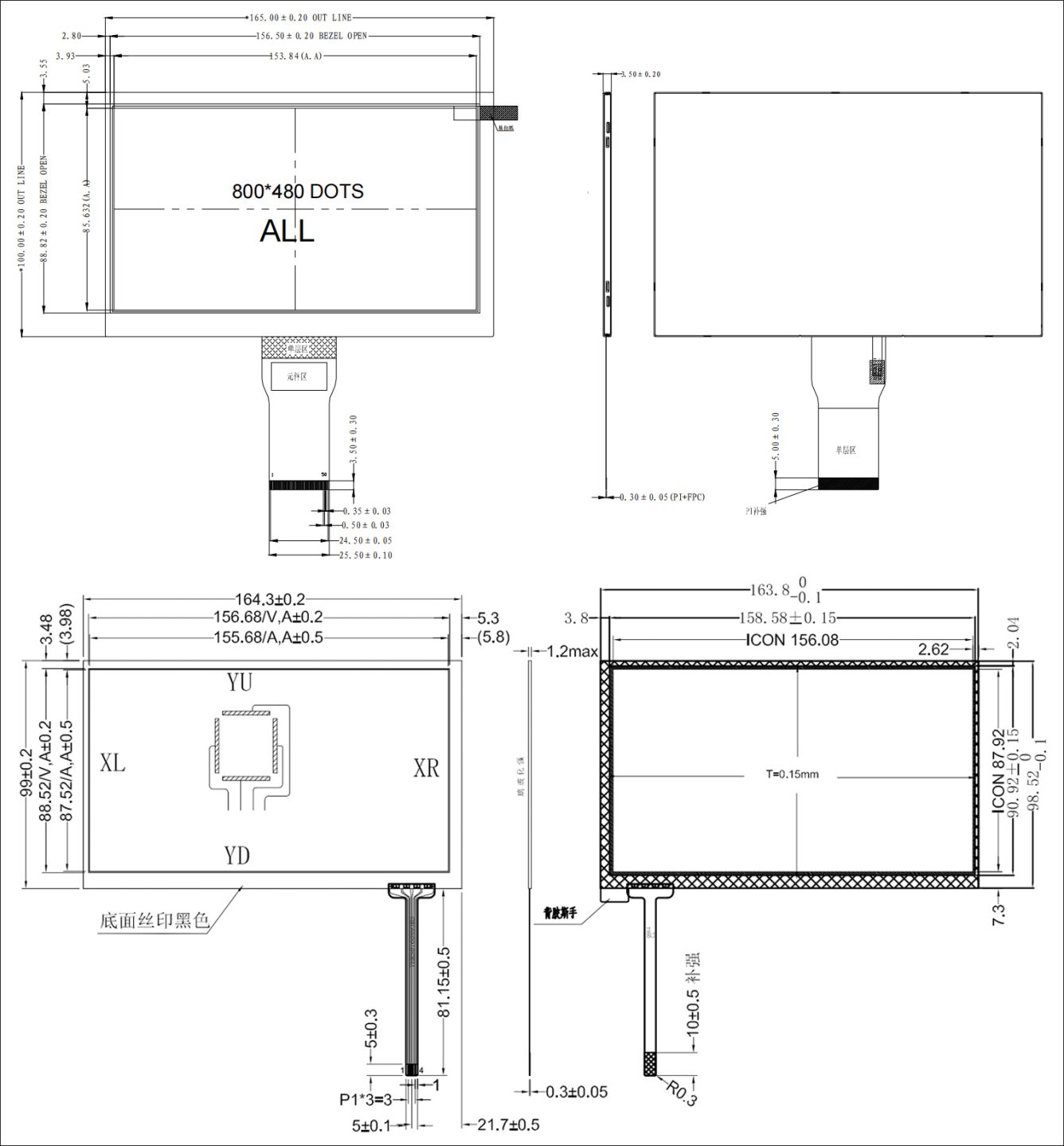
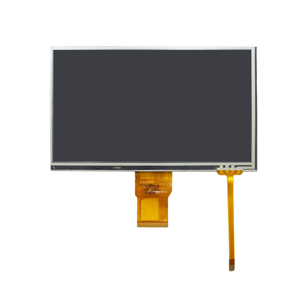

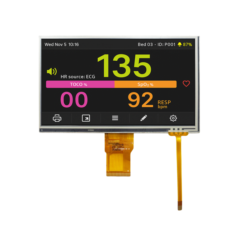
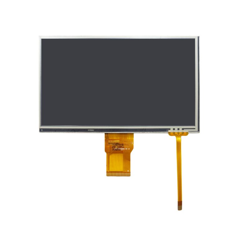

| PIN NO. | SYMBOL | DESCRIPTION |
| 1~2 | VLED+ | Power for LED backlight (Anode) |
| 3~4 | VLED- | Power for LED backlight (Cathode) |
| 5 | GND | Power ground |
| 6 | VCOM | Common Voltage |
| 7 | DVDD | Digital Power |
| 8 | MODE | DE/SYNC mode select. |
| 9 | DE | Data Enable signal |
| 10 | VSYNC | Vertical sync input |
| 11 | HSYNC | Horizontal sync input |
| 12 | B7 | Blue data (MSB) |
| 13~18 | B6~B1 | Blue data |
| 19 | B0 | Blue data (LSB) |
| 20 | G7 | Green data (MSB) |
| 21~26 | G6~G1 | Green data |
| 27 | G0 | Green data (LSB) |
| 28 | R7 | Red data (MSB) |
| 29~34 | R6 | Red data |
| 35 | R0 | Red data (LSB) |
| 36 | GND | Power ground |
| 37 | DCLK | Clock input |
| 38 | GND | Power ground |
| 39 | SHLR | Left/Right Selection |
| 40 | UPDN | Up/Down Selection |
| 41 | VGH | Gate ON Voltage |
| 42 | VGL | Gate OFF Voltage |
| 43 | AVDD | Power for Analog Circuit |
| 44 | RESET | Global reset pin |
| 45 | NC | Not connection |
| 46 | VCOM | Common Voltage |
| 47 | DITH | Dithering function enable control |
| 48 | GND | Power ground |
| 49~50 | NC | Not connection |
| PIN NO. | OUT |
| 1 | XL |
| 2 | YD |
| 3 | XR |
| 4 | YU |
| Item | Symbol | Min. | Max. | Unit |
| Digital Supply Voltage | VDD | -0.3 | 3.6 | V |
| Analog Supply Voltage | AVDD | -0.5 | 14.85 | V |
| TFT Gate ON Voltage | VGH | 0.3 | 20 | V |
| TFT Gate OFF Voltage | VGL | -20 | 0.3 | V |
| TFT Common Electrode Voltage | VCOM | 0 | 6 | V |
| Operating Temperature | TOP | -20 | 70 | ℃ |
| Storage Temperature | TST | -30 | 80 | ℃ |
| Item | Symbol | Min. | Typ | Max. | Unit |
| Digital Supply Voltage | VDD | 3.0 | 3.3 | 3.6 | V |
| Analog Supply Voltage | AVDD | - | 10 | - | V |
| TFT Gate ON Voltage | VGH | 16.5 | 17.0 | 17.5 | V |
| TFT Gate OFF Voltage | VGL | -11.5 | -11 | -10.5 | V |
| TFT Common Electrode Voltage | VCOM | -0.5 | 0 | 0.5 | V |