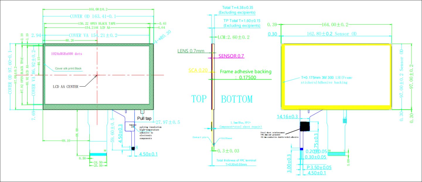


| PIN NO. | Symbol | Functional |
| 1 | LED A | LED Anode |
| 2 | LED A | LED Anode |
| 3 | LED K | LED Cathode |
| 4 | LED K | LED Cathode |
| 5 | GND | Digital Ground |
| 6 | VCOM | For external VCOM DC input |
| 7 | DVDD | Digital Power |
| 8 | MODE | DE/SYNC mode select MODE=H:DE mode(normally pull high) MODE=L:HSD/VSD mode |
| 9 | DE | Data enable signal |
| 10 | VSYNC | Vertical sync input. Negative polarity |
| 11 | HSYNC | Horizontal sync input. Negative polarity |
| 12~19 | B7~B0 | Blue data Input |
| 20~27 | G7~G0 | Green data Input |
| 28~35 | R7~R0 | Red data Input |
| 36 | GND | Digital Ground |
| 37 | DCLK | Clock input |
| 38 | GND | Digital Ground |
| 39 | L/R | Source right or left sequence control SHLR=H:right shift, Left→Right SHLR=L:left right, Right→Left |
| 40 | U/D | Gate up or down scan control UPDN=H:up shift, Down→Up UPDN=L:down shift, Up→Down |
| 41 | VGH | Positive Power for TFT |
| 42 | VGL | Negative Power for TFT |
| 43 | AVDD | Analog Power |
| 44 | RSTB | Global reset pin. Active low to enter reset state Suggest to connecting with an RC reset circuit for stability. Normally pull high. (RC circuit: R=10KΩ, C=1uF) |
| 45 | NC | Not connect |
| 46 | VCOM | For external VCOM DC input |
| 47 | DITHB | Dithering setting |
| 48 | GND | Digital Ground |
| 49~50 | NC | Not connect |
| PIN NO. | Assignment |
| 1 | GND |
| 2 | SCL |
| 3 | SDA |
| 4 | INT |
| 5 | RST |
| 6 | NC |
| 7 | VDD |
| 8 | NC |
| Parameter | Symbol | Min | Max | Unit |
| Power supply1 | VDD | -0.5 | +3.96 | V |
| Power supply2 |
AVDD |
-0.5 | +13.85 | V |
| Operating temperature |
TOPR |
-10 | 50 | ℃ |
| Storage temperature |
TSTG |
-20 | 60 | ℃ |
| Item | Symbol | Min | Typical | Max | Unit |
| LED module Forward voltage |
VLED |
9.0 | 9.3 | 9.6 | V |
| LED module current |
ILED |
- | 140 | - | mA |
| LCM Surface Luminance ★1 |
LS |
- | 300 | - |
cd/m2 |
| LCM Surface brightness uniform ★2 |
LD |
80 | - | - | % |