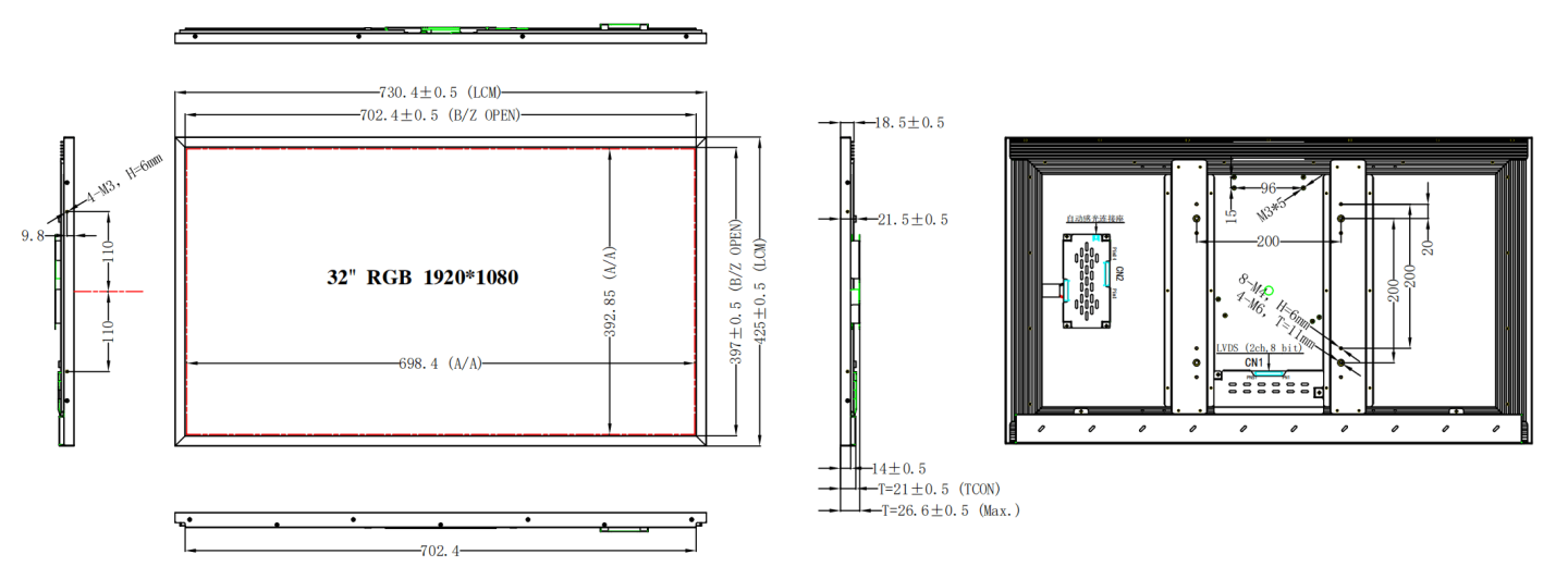


| PIN NO. | Symbol | Description | PIN NO. | Symbol | Description |
| 1 | NC | No Connection (Note 4) | 27 | NC | No connection |
| 2 | NC | No Connection (Note 4) | 28 | R2AN | SECOND LVDS Receiver Signal (A-) |
| 3 | NC | No Connection (Note 4) | 29 | R2AP | SECOND LVDS Receiver Signal (A+) |
| 4 | NC | No Connection (Note 4) | 30 | R2BN | SECOND LVDS Receiver Signal (B-) |
| 5 | NC | No Connection (Note 4) | 31 | R2BP | SECOND LVDS Receiver Signal (B+) |
| 6 | NC | No Connection (Note 4) | 32 | R2CN | SECOND LVDS Receiver Signal (C-) |
| 7 | LVDS Select | ‘H’=JEIDA , ‘L’or NC= VESA | 33 | R2CP | SECOND LVDS Receiver Signal (C+) |
| 8 | NC | No Connection (Note 4) | 34 | GND | Ground |
| 9 | NC | No Connection (Note 4) | 35 | R2CLKN | SECOND LVDS Receiver Clock Signal(-) |
| 10 | NC | No Connection (Note 4) | 36 | R2CLKP | SECOND LVDS Receiver Clock Signal(+) |
| 11 | GND | Ground | 37 | GND | Ground |
| 12 | R1AN | FIRST LVDS Receiver Signal (A-) | 38 | R2DN | SECOND LVDS Receiver Signal (D-) |
| 13 | R1AP | FIRST LVDS Receiver Signal (A+) | 39 | R2DP | SECOND LVDS Receiver Signal (D+) |
| 14 | R1BN | FIRST LVDS Receiver Signal (B-) | 40 | NC | No connection |
| 15 | R1BP | FIRST LVDS Receiver Signal (B+) | 41 | NC | No connection |
| 16 | R1CN | FIRST LVDS Receiver Signal (C-) | 42 | NC or GND | No Connection or Ground |
| 17 | R1CP | FIRST LVDS Receiver Signal (C+) | 43 | NC or GND | No Connection or Ground |
| 18 | GND | Ground | 44 | GND | Ground (Note 5) |
| 19 | R1CLKN | FIRST LVDS Receiver Clock Signal(-) | 45 | GND | Ground |
| 20 | R1CLKP | FIRST LVDS Receiver Clock Signal(+) | 46 | GND | Ground |
| 21 | GND | Ground | 47 | NC | No connection |
| 22 | R1DN | FIRST LVDS Receiver Signal (D-) | 48 | VLCD | Power Supply +12.0V |
| 23 | R1DP | FIRST LVDS Receiver Signal (D+) | 49 | VLCD | Power Supply +12.0V |
| 24 | NC | No connection | 50 | VLCD | Power Supply +12.0V |
| 25 | NC | No connection | 51 | VLCD | Power Supply +12.0V |
| 26 | NC or GND | No Connection or Ground | - | - | - |
| Parameter | Symbol | Value | Unit | Note | ||
| Min | Max | |||||
| Power Input Voltage | LCD Circuit |
VLCD |
-0.3 | +14.0 | V | 1 |
| T-Con Option Selection Voltage |
VLOGIC |
-0.3 | +4.0 | V | ||
| Operating Temperature |
TOP |
-20 | +80 | ℃ | 2,3 | |
| Storage Temperature (without packing) |
TST |
-20 | +80 | ℃ | ||
| Panel Front Temperature (Considering L/C Phase Transition Temperature) |
TPT |
— | +80 | ℃ | 4 | |
| Operating Ambient Humidity |
HOP |
10 | 90 | %RH | 2,3 | |
| Storage Humidity |
HST |
5 | 90 | %RH | ||
Note:
-
Ambient temperature condition: Ta = 25 ± 2 ℃.
-
Temperature and relative humidity ranges are shown in the figure below. The maximum wet-bulb temperature should be 39 ℃, and no condensation of water is allowed.
-
Gravity mura can be guaranteed below 80 ℃ and under backlight luminance of 1000 nit.
-
The maximum operating temperature is based on the test condition that the surface temperature of the display area is ≤ 80 ℃ with the LCD module alone in a temperature-controlled chamber. Thermal management should be considered in the final product design to prevent the surface temperature of the display area from exceeding 80 ℃. The range of operating temperature may be degraded in case of improper thermal management in the final product design.
-
Prevent products from being exposed to direct sunlight; otherwise, reliability and function may not be guaranteed.
| Parameter | Symbol | Value | Unit | Note | |||
| Min | Typ | Max | |||||
| Power Input Voltage | VLCD | 10.8 | 12.0 | 13.2 | V | 4 | |
| Power Input Current | ILCD | — | 380 | 495 | mA | 1 | |
| — | 505 | 660 | mA | 2 | |||
| T-CON Option Selection Voltage | Input High Voltage | VIH | 2.7 | — | 3.6 | V | — |
| Input Low Voltage | VIL | 0 | — | 0.7 | V | — | |
| Power Consumption | PLCD | — | 4.6 | 5.98 | W | 1 | |
| — | 6.1 | 7.93 | W | 2 | |||
| Rush current | IRUSH | — | — | 5.0 | A | 3 | |
Note:
- The specified current and power consumption are under the VLCD=12.0V, Ta=25±2℃, fV=60Hz condition, and mosaic pattern (8×6) is displayed and fV is the frame frequency.
- The current and power consumption are specified at the maximum current patter.
- The duration of rush current is about 2ms and rising time of power input is 0.5ms(min.).
- Ripple voltage level is recommended under ±5% of typical voltage.
| PIN# | Symbol | Description |
| 1 | VDDB | Operating Voltage Supply,+24V DC Regulated |
| 2 | VDDB | Operating Voltage Supply,+24V DC Regulated |
| 3 | VDDB | Operating Voltage Supply,+24V DC Regulated |
| 4 | VDDB | Operating Voltage Supply,+24V DC Regulated |
| 5 | VDDB | Operating Voltage Supply,+24V DC Regulated |
| 6 | GND | Ground |
| 7 | GND | Ground |
| 8 | GND | Ground |
| 9 | GND | Ground |
| 10 | GND | Ground |
| 11 | Not connect | |
| 12 | VBLON | BL On-Off: High (2.5~5.5V) for BL, Low/Open (0~0.5V) for BL off. |
| 13 | VDIM (note 1) | Internal DC Dimming High (3.3V/100%Duty) for 100%Lum |
| 14 | PWM | Internal PWM Dimming |
Note 1: DC dimming function is included internal DC and external DC.
Internal DC: input voltage 0 (GND) ~3.3V to pin 13th, and duty ratio of output voltage/current of inverter is from 30% to 100%. When use pin 13th to control backlight luminance, the pin 14th will be PWM.