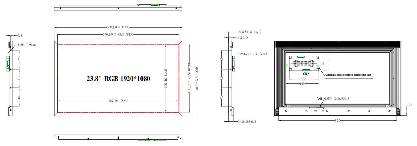


| Pin No. | Symbol | Description |
| 1 | NC | No Connection |
| 2 | SDA_VCOM | I²C Data (BOE Use Only) |
| 3 | SCL_VCOM | PC Clock (BOE Use Only) |
| 4~5 | NC | Not Connected |
| 6 | SDA_EEPROM | I²C Data for EEPROM |
| 7 | SCL_EEPROM | I²C Clock for EEPROM |
| 8 | WP_EEPROM | H: EEPROM Write Disable (Default); L: EEPROM Write Enable |
| 9 | NC | Not Connected |
| 10~11 | GND | Ground |
| 12 | CH1[0]- | Negative LVDS differential data input. Pair 0 (ODD) |
| 13 | CH1[0]+ | Positive LVDS differential data input. Pair 0 (ODD) |
| 14 | CH1[1]- | Negative LVDS differential data input. Pair 1 (ODD) |
| 15 | CH1[1]+ | Positive LVDS differential data input. Pair 1 (ODD) |
| 16 | CH1[2]- | Negative LVDS differential data input. Pair 2 (ODD) |
| 17 | CH1[2]+ | Positive LVDS differential data input. Pair 2 (ODD) |
| 18 | GND | Ground |
| 19 | CH1CLK- | Negative LVDS clock (ODD) |
| 20 | CH1CLK+ | Positive LVDS clock (ODD) |
| 21 | GND | Ground |
| 22 | CH1[3]- | Negative LVDS differential data input. Pair 3 (ODD) |
| 23 | CH1[3]+ | Positive LVDS differential data input. Pair 3 (ODD) |
| 24~27 | NC | Not Connected |
| 28 | CH2[0]- | Negative LVDS differential data input. Pair 0 (EVEN) |
| 29 | CH2[0]+ | Positive LVDS differential data input. Pair 0 (EVEN) |
| 30 | CH2[1]- | Negative LVDS differential data input. Pair 1 (EVEN) |
| 31 | CH2[1]+ | Positive LVDS differential data input. Pair 1 (EVEN) |
| 32 | CH2[2]- | Negative LVDS differential data input. Pair 2 (EVEN) |
| 33 | CH2[2]+ | Positive LVDS differential data input. Pair 2 (EVEN) |
| 34 | GND | Ground |
| 35 | CH2CLK- | Negative LVDS clock (EVEN) |
| 36 | CH2CLK+ | Positive LVDS clock (EVEN) |
| 37 | GND | Ground |
| 38 | CH2[3]- | Negative LVDS differential data input. Pair 3 (EVEN) |
| 39 | CH2[3]+ | Positive LVDS differential data input. Pair 3 (EVEN) |
| 40~43 | NC | Not Connected |
| 44~46 | GND | Ground |
| 47 | NC | Not Connected |
| 48~51 | VCC | Input Voltage +5V |
| Pin | Symbol | Description |
| 1 | VDDB | Power Supply Input Voltage |
| 2 | VDDB | Power Supply Input Voltage |
| 3 | VDDB | Power Supply Input Voltage |
| 4 | VDDB | Power Supply Input Voltage |
| 5 | VDDB | Power Supply Input Voltage |
| 6 | GND | Ground |
| 7 | GND | Ground |
| 8 | GND | Ground |
| 9 | GND | Ground |
| 10 | GND | Ground |
| 11 | NC | NC |
| 12 | VBLON | BLU On-Off control |
| 13 | PDIM | Extermal DC |
| 14 | PDIM | External PWM (High (3.3V/100% Duty)for 100% Lum) |
| Parameter | Symbol | Min. | Max. | Unit | Remarks |
| Power Supply Voltage |
VDD |
-0.3 | 6.0 | V | Ta=25℃ |
| Logic Supply Voltage |
VIN |
VSS-0.3 |
VDD+0.3 |
V | |
| Operating Temperature |
TOP |
-20 | +70 | ℃ | 1) |
| Storage Temperature |
TST |
-30 | +70 | ℃ | 1) |
| LCM Surface Temperature(Operation) |
Tsurface |
0 | +70 | ℃ | 2) |
Note:
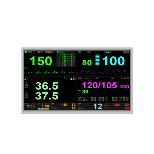
1) Temperature and relative humidity range are shown in the figure below. Wet bulb temperature should be 39℃ max. and no condensation of water.
2) Panel Surface Temperature should be Min.0℃ and Max.+75℃ under the VDD=5.0V, Frame rate=60Hz, 25℃ ambient Temp. no humidity control and LED string current is typical value.
| Parameter | Min. | Typ. | Max. | Unit | Remarks | |
| Power Supply Voltage |
VDD |
4.5 | 5.0 | 5.5 | V | Note l |
| Power Supply Ripple Voltage |
VRP |
— | — | 250 | mV | |
| Power Supply Current |
IDD |
— | 1200 | 1600 | mA | |
| Power Consumption |
PD |
— | 6.0 | 8.0 | W | — |
| In-Rush Current |
IRUSH |
— | 2.0 | 3.0 | A | Note 2 |
| Permissible Input Ripple Voltage |
VRF |
— | — | 300 | mV | Note 1,3 |
| High Level Differential Input Threshold Voltage |
VIH |
— | — | +100 | mV | — |
| Low Level Differential Input Threshold Voltage |
VIL |
-100 | — | — | mV | |
| Differential Input Voltage |
|VID| |
200 | — | 600 | mV | — |
| Differential Input Common Mode Voltage |
Vcm |
1.0 | 1.2 | 1.5 | — |
VIH=100mV, VIL=-100mV |
Notes:
1. The supply voltage is measured and specified at the interface connector of LCM. The current draw and power consumption specified is for VDD=5.0V, Frame rate=60Hz, Clock frequency =74.25MHz.
2. Duration of rush current is about 2 ms and rising time of VDD is 520μs±20%.
3. Ripple Voltage should be covered by Input voltage Spec.
4. Calculated value for reference (Input pins*VPIN×IPIN) excluding inverter loss.
| Item | Symbol | Min | Typ | Max | Unit | Note | |
| Power Supply Input Voltage |
VDDB |
22.8 | 24 | 25.2 | V | — | |
| Power Supply Input Current |
IDDB |
— | 2.00 | — | A | VDDB=24V | |
| Power Consumption |
PDDB |
— | 48.0 | — | Watt | ||
| Inrush Current |
IRUSH |
— | — | 16.1 | A | ||
| Control signal voltage |
Vsignal |
High | 2 | — | 5.5 | V | |
| Low | 0 | — | 0.8 | ||||
| Control signal current |
Isignal |
— | — | 1.5 | mA | ||
| External PWM Duty ratio (input duty ratio) | D_EPWM | 0 | — | 100 | % | ||
| External PWM Frequency |
F_EPWM | 100 | — | 1000 | Hz | ||
| External DC Duty ratio (input duty ratio) |
D_E DC | 25 | — | 100 | % | ||
| External DC Voltage | V_E DC | 0 | — | 5.0 | V | ||
| External induction dimming | (Duty ratio) | 25 | — | 100 | % | ||
| Input Impedance |
Rin |
300 | — | — | Kohm | ||
| LED lifetime |
LTLED |
50,000 | — | — | Hr | — | |