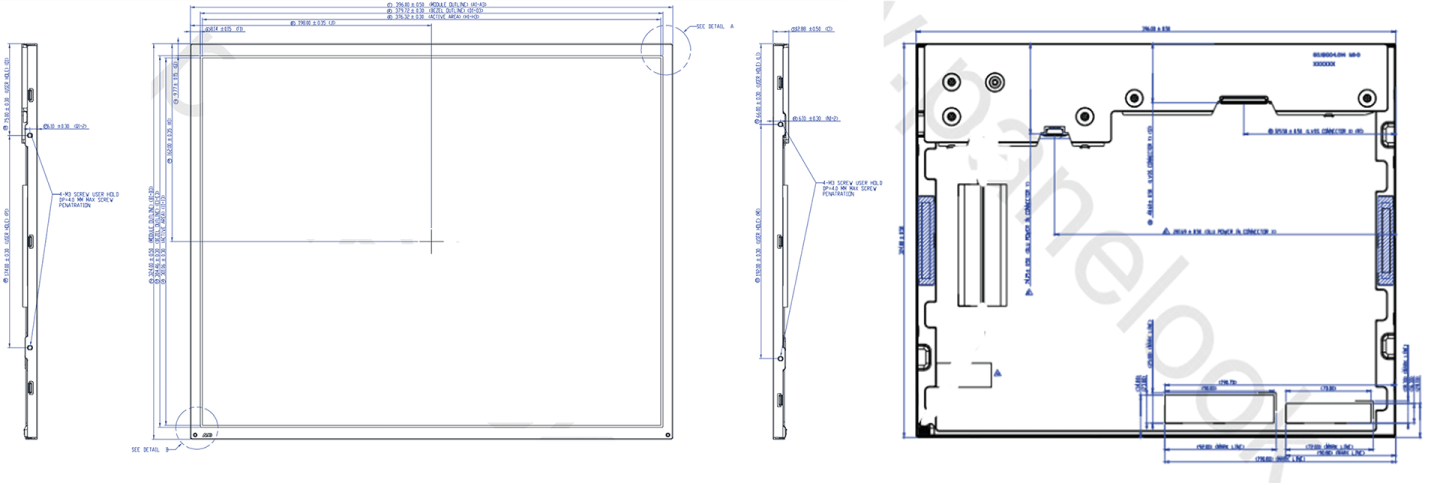


| PIN# | SIGNAL NAME | DESCRIPTION |
| 1 | RxOINO- | Negative LVDS differential data input (Odd data) |
| 2 | RxOINO+ | Positive LVDS differential data input (Odd data) |
| 3 | RxOIN1- | Negative LVDS differential data input (Odd data) |
| 4 | RxOIN1+ | Positive LVDS differential data input (Odd data) |
| 5 | RxOIN2- | Negative LVDS differential data input (Odd data, DSPTMG) |
| 6 | RxOIN2+ | Positive LVDS differential data input (Odd data, DSPTMG) |
| 7 | GND | Power Ground |
| 8 | RxOCLKIN- | Negative LVDS differential clock input (Odd clock) |
| 9 | RxOCLKIN+ | Positive LVDS differential clock input (Odd clock) |
| 10 | RxOIN3- | Negative LVDS differential data input (Odd data) |
| 11 | RxOIN3+ | Positive LVDS differential data input (Odd data) |
| 12 | RxEINO- | Negative LVDS differential data input (Even data) |
| 13 | RxEINO+ | Positive LVDS differential data input (Even data) |
| 14 | GND | Power Ground |
| 15 | RxEIN1- | Negative LVDS differential data input (Even data) |
| 16 | RxEIN1+ | Positive LVDS differential data input (Even data) |
| 17 | GND | Power Ground |
| 18 | RxEIN2- | Negative LVDS differential data input (Even data) |
| 19 | RxEIN2+ | Positive LVDS differential data input (Even data) |
| 20 | RxECLKIN- | Negative LVDS differential clock input (Even clock) |
| 21 | RxECLKIN+ | Positive LVDS differential clock input (Even clock) |
| 22 | RxEIN3- | Negative LVDS differential data input (Even data) |
| 23 | RxEIN3+ | Positive LVDS differential data input (Even data) |
| 24 | GND | Power Ground |
| 25 | GND | Power Ground |
| 26 | GND | Power Ground |
| 27 | GND | Power Ground |
| 28 | POWER | Power+5V |
| 29 | POWER | Power +5V |
| 30 | POWER | Power +5V |
| Note: "Power Ground" stands for 0V. | ||
| Pin No. | Symbol | Description |
| 1 | VCC | Power supply voltage +12V |
| 2 | VCC | Power supply voltage +12V |
| 3 | ON/OFF | Output enable signal |
| 4 | DIM | Dimming signal |
| 5 | GND | Power ground |
| 6 | GND | Power ground |
PH2.0-6 (2.0mmX6)
| Item | Symbol | Min. | Max. | Unit |
| Logic/LCD Drive Voltage |
VDD |
-0.3 | 6 | [Volt] |
| Operating Temperature |
TOP |
-30 | +85 | [℃] |
| Operation Humidity |
HOP |
5 | 95 | [%RH] |
| Storage Temperature |
TST |
-30 | +85 | [℃] |
| Storage Humidity |
HST |
5 | 95 | [%RH] |
| Symbol | Parameter | Min | Typ | Max | Unit | Conditions |
| VDD | Logic/LCD Drive Voltage |
4.5 | 5 | 5.5 | [Volt] | +/-10% |
| IDD | Input Current | — | 1 | 1.2 | [A] | VDD=5.0V, All Black Pattern At 75Hz |
| PDD | VDD Power | — | 5 | 6 | [Watt] | VDD=5.0V, All Black Pattern At 75Hz |
| IRush | Inrush Current | — | — | 3 | [A] | — |
| VDDrp | Allowable Logic/LCD Drive Ripple Voltage | — | — | 100 | [mV]p-p | VDD=5.0V, All Black Pattern At 75Hz |
| Symbol | Parameter | Min. | Typ. | Max. | Unit | Remark |
| VCC | Input Voltage | 10.8 | 12 | 13.4 | [Volt] | — |
|
lVCC |
Input Current | — | — | 2.15 | [A] | Ta=25℃ RMS+Ripple Value, at 100% PWM |
|
PVCC |
Power Consumption | — | 15 | 18.7 | [Watt] | 100% PWM Duty |
|
FPWM |
Dimming Frequency | 200 | — | 20K | [Hz] | — |
| Swing Voltage | 3 | 3.3 | 5 | [Volt] | — | |
| Dimming duty cycle | 5 | — | 100 | % | — | |
|
VLED ON/OFF |
On Control Voltage | 3 | 3.3 | 5 | [Volt] | — |
| Off Control Voltage | 0 | 0 | 0.8 | [Volt] | ||
|
IF |
LED Forward Current | — | 100 | — | [mA] | Ta=25℃ |
|
VF |
LED Forward Voltage | 33.6 | 38.4 | 43.2 | [Volt] |
IF=100mA, Ta=25℃ |
|
PLED |
LED Power Consumption | — | — | 20 | [Watt] | |
| LED Life Time | — | 50000 | — | Hrs |