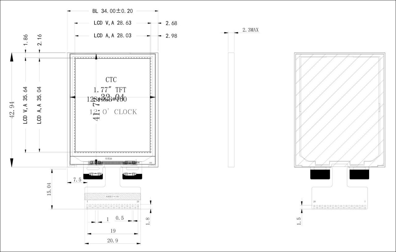
| PIN NO. | Symbol | Description |
| 1 | LEDK | Back-light Cathode |
| 2 | LEDA | Back-light Anode |
| 3 | GND | Power Ground |
| 4 | VCC | Power supply for interface logic circuits(2.8V-3.2V) |
| 5~6 | NC | NC |
| 7 | CS | Chip select input pin |
| 8 | RSTB | Reset input pin |
| 9 | RS | Data or Command select pin in the parallel interface |
| 10 | WR | Write signal input pin |
| 11 | RD | Serial output signal |
| 12-19 | DB7~DBO | Data bus for MCU |
| 20 | GND | Power Ground |
| Characteristics | Symbol | Min. | Max. | Unit |
| Supply Voltage | IOVCC | -0.3 | 4.6 | V |
| VCI | -0.3 | 4.8 | V | |
| TFT Gate On Voltage | VGH | -0.3 | 30 | V |
| TFT Gate Off Voltage | VGL | -0.3 | 30 | V |
| Backlight Forward Current | lF | - | 40 | mA |
| Operating Temperature | Topr | -20 | +70 | ℃ |
| Storage Temperature | Tstg | -30 | +80 | ℃ |
| Humidity | RH | - | 90 | % |
| Characteristics | Symbol | Min. | Typ. | Max. | Unit | Note |
| Power Supply Voltage 1 |
IOVCC |
1.65 | 1.8 | 3.7 | V | - |
| Power Supply Voltage 2 | VCI | 2.5 | 2.75 | 4.8 | V | - |
| Input voltage “L” Level |
VIL |
GND | - | 0.3IOVCC | V | IOVCC=1.65~3.3V |
| Input voltage “H” Level |
VIH |
0.7IOVCC | - | IOVCC | V | |
| Output voltage “L” Level |
VOL |
GND | - | 0.2IOVCC | V |
lOL=1mA |
| Output voltage “H” Level |
VOH |
0.8IOVCC | - | IOVCC | V |
lOH=-1mA |
| Characteristics | Symbol | Condition | Min. | Type | Max. | Unit |
| Forward Voltage |
VF |
IL=40mA | 2.8 | 3.0 | 3.2 | V |
| Forward Current |
IL |
- | - | 40 | - | mA |
| Luminance |
LV |
IL=40mA | TBD | 250 | - | cd/m² |
| LED Life Time | - | IL=40mA | 20,000 | 25,000 | - | Hr |