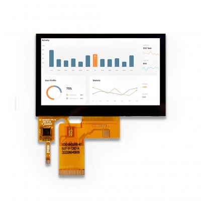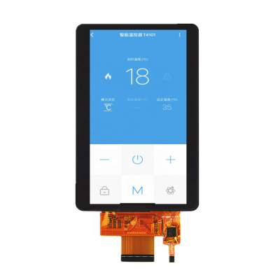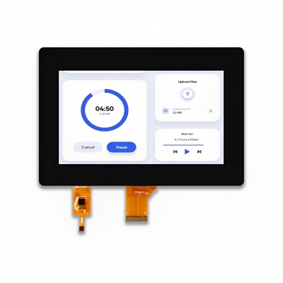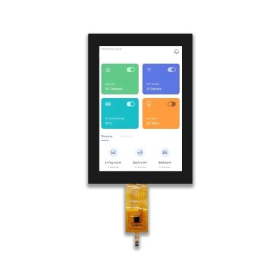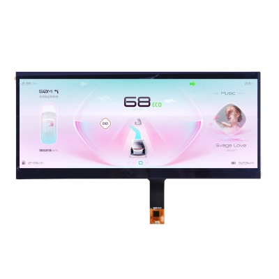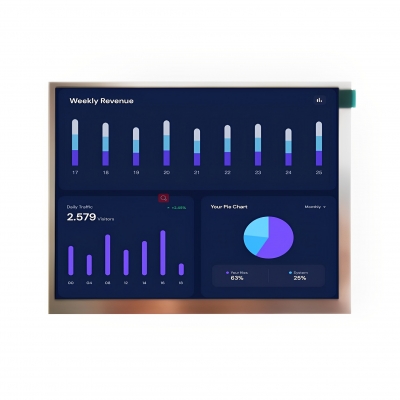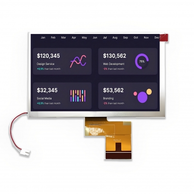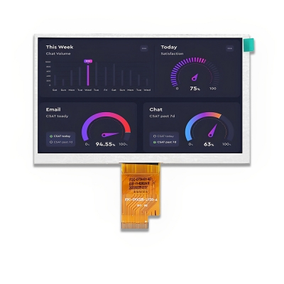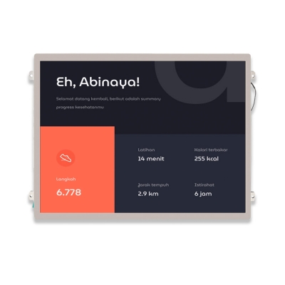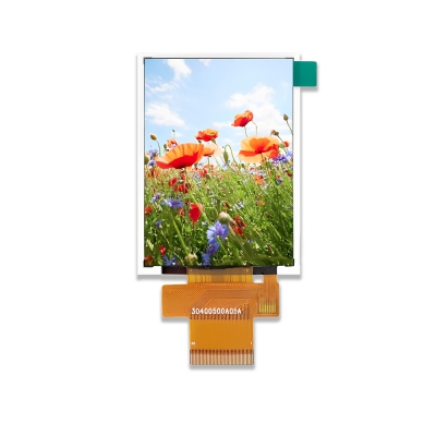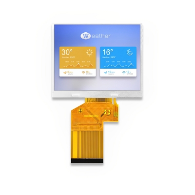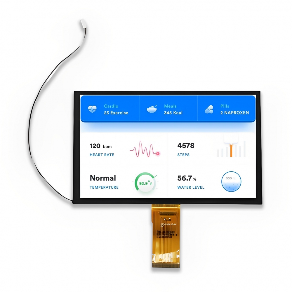

Product Structure
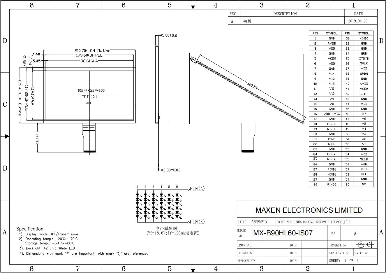
LCD PIN Function
|
Pin NO. |
Symbol |
Description |
|
1 |
GND |
Ground |
|
2 |
AVDD |
Analog Power |
|
3 |
VDD |
Digital Power |
|
4 |
GND |
Ground |
|
5 |
VCOM |
Common voltage |
|
6 |
VDD |
Digital Power |
|
7 |
GND |
Ground |
|
8~14 |
V14~V8 |
Gamma correction voltage reference |
|
15 |
GND |
Ground |
|
16 |
VDD_LVDS |
LVDS Power |
|
17 |
GND |
Ground |
|
18 |
PIND3 |
Positive LVDS Differential Data Inputs |
|
19 |
NIND3 |
Negative LVDS Differential Data Inputs |
|
20 |
GND |
Ground |
|
21 |
PINC |
Positive LVDS Differential Clock Inputs |
|
22 |
NINC |
Negative LVDS Differential Clock Inputs |
|
23 |
GND |
Ground |
|
24 |
PIND2 |
Positive LVDS Differential Data Inputs |
|
25 |
NIND2 |
Negative LVDS Differential Data Inputs |
|
26 |
GND |
Ground |
|
27 |
PIND1 |
Positive LVDS Differential Data Inputs |
|
28 |
NIND1 |
Negative LVDS Differential Data Inputs |
|
29 |
GND |
Ground |
|
30 |
PIND0 |
Positive LVDS Differential Data Inputs |
|
31 |
NIND0 |
Negative LVDS Differential Data Inputs |
|
32 |
GND |
Ground |
|
33 |
GND |
Ground |
|
34 |
GRB |
Global reset pin. Active Low to enter Reset State. Normally pull high. It’s necessary to connecting with an RC delay circuit for stability. (GRB delay VDD larger than 1ms) |
|
35 |
STBYB |
Standby mode, normally pull high STBYB=”1”, Normal Operation STBYB=”0”,Timing control, source driver will turn off, all output are high-Z |
|
36 |
SHLR |
Horizontal Inversion |
|
37 |
VDD |
Digital Power |
|
38 |
UPDN |
Vertical Inversion |
|
39 |
GND |
Ground |
|
40 |
AVDD |
Analog Power |
|
41 |
VCOM |
Common voltage |
|
42 |
DITH |
Dithering function |
|
43 |
GND |
Ground |
|
44 |
VDD |
Digital Power |
|
45 |
GND |
Ground |
|
46~52 |
V7~V1 |
Gamma correction voltage reference |
|
53 |
GND |
Ground |
|
54 |
VDD |
Digital Power |
|
55 |
SELB |
6 bit/8 bit mode select |
|
56 |
VGH |
Positive Power for TFT |
|
57 |
VDD |
Digital Power |
|
58 |
VGL |
Negative Power for TFT |
|
59 |
GND |
Ground |
|
60 |
NC |
No connection |
|
Parameter |
Symbol |
Min. |
Typ. |
Max. |
Unit |
Note |
|
Power supply |
VDD |
-0.3 |
- |
3.96 |
V |
|
|
AVDD |
-0.5 |
- |
14.85 |
V |
|
|
|
VGL |
-20 |
- |
0.3 |
V |
|
|
|
VGH |
-0.3 |
|
42 |
V |
|
|
|
Operating Temperature |
TOP |
-20 |
- |
70 |
℃ |
|
|
Storage Temperature |
TST |
-30 |
- |
80 |
℃ |
|
|
Item |
Storage |
Operating |
Note |
||
|
MIN. |
MAX. |
MIN. |
MAX. |
||
|
Ambient Temperature |
-30℃ |
80℃ |
-20℃ |
70℃ |
1,2 |
|
Parameter |
Symbol |
Min. |
Typ. |
Max. |
Unit |
Note |
|
|
Power supply |
VDD |
3 |
3.3 |
3.6 |
V |
|
|
|
AVDD |
9.6 |
10.2 |
13.5 |
V |
|
||
|
VGL |
|
-8 |
|
V |
|
||
|
VGH |
|
18 |
|
V |
|
||
|
Input signal voltage |
VCOM |
4 |
4.4 |
4.6 |
|
|
|
|
Input voltage |
‘H’ |
VIH |
0.7VVDD |
- |
VVDD |
V |
|
|
‘L’ |
VIL |
0 |
- |
0.3VVDD |
V |
|
|
|
Item |
Symbol |
Condition |
Min. |
Typ. |
Max. |
Unit |
Note |
|
Supply voltage |
Vf |
- |
16.8 |
18.6 |
20.4 |
V |
1 |
|
Supply current |
If |
- |
- |
120 |
- |
mA |
2 |
|
Number of LED |
- |
6Sx6P |
- |
36 |
- |
Piece |
|
|
Power Consumption |
- |
- |
2016 |
2232 |
2448 |
mW |
|
|
LED life time |
- |
- |
30000 |
- |
- |
Hrs |
|