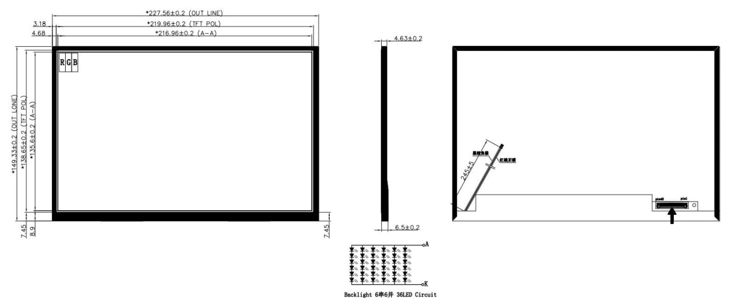

| Pin No. | Symbol | Description | I/O |
| 1 | NC | Non Connection | - |
| 2~4 | VDDIN | Power supply VDDIN=3.3V(Typ.) | P |
| 5 | NC | Non Connection | - |
| 6~7 | GND | GROUND | P |
| 8 | RINO- | LVDS Negative data signal (-) | I |
| 9 | RINO+ | LVDS Positive data signal(+) | I |
| 10 | GND | GROUND | P |
| 11 | RIN1- | LVDS Negative data signal (-) | I |
| 12 | RIN1+ | LVDS Positive data signal(+) | I |
| 13 | GND | GROUND | P |
| 14 | RIN2- | LVDS Negative data signal (-) | I |
| 15 | RIN2+ | LVDS Positive data signal(+) | I |
| 16 | GND | GROUND | P |
| 17 | LVDS_CLK- | LVDS Negative CLK signal (-) | I |
| 18 | LVDS_CLK+ | LVDS Positive CLK signal(+) | I |
| 19 | GND | GROUND | P |
| 20 | RIN3- | LVDS Negative data signal (-) | I |
| 21 | RIN3+ | LVDS Positive data signal(+) | I |
| 22 | GND | GROUND | P |
| 23~24 | NC | Non Connection | - |
| 25 | GND | GROUND | P |
| 26 | SCL_S | Reserved for LCD manufacturer's use, not connection | - |
| 27 | SDA_S | Reserved for LCD manufacturer’s use, not connection | - |
| 28 | GND | GROUND | P |
| 29 | NC | Non Connection | - |
| 30 | NC | Non Connection | - |
| 31~33 | GND | GROUND | P |
| 34 | NC | Non Connection | - |
| 35 | LED_PWM | LED PWM signal pin | O |
| 36~37 | NC | Non Connection | - |
| 38~40 | LED+ | LED Anode | P |
| Parameter | Symbol | Min. | Max. | Unit | Remarks |
| Power Supply | VDD | VSS-0.3 | 3.6 | V | Ta =25℃ Note 1&2 |
| Operating Temperature | Top | -20 | +70 | ℃ | _ |
|
Storage Temperature |
TsT | -30 | +80 | ℃ |
Note:
1. These range above is maximum value not the actual operating temperature. Actual Operating temperature is no more than 40℃ and temperature refers to the LCM surface temperature;
2.MAXEN is not responsible for product problems beyond the use conditions.
| Parameter | Symbol | Values | Unit | Notes | |||
| Min. | Typ. | Max. | |||||
| Power Supply Voltage | VDD | 3.0 | 3.3 | 3.6 | V | - | |
| VRP | - | - | 360 | mV | Ripple | ||
| Power Supply Current | IDD | - | 127 | 343 | mA | Note 1 | |
| Power Consumption | PLCD | - | 0.42 | 1.13 | W | ||
| Rush current | IRUSH | - | - | 3.0 | A | - | |
| CMOS Interface |
Input Voltage |
VIH | 2.7 | - | 3.3 | V | - |
| VIL | 0 | - | 0.5 | V | - | ||
| Output Voltage |
VOH | 2.7 | - | 3.3 | V | - | |
| VOL | 0 | - | 0.5 | V | - | ||
Notes:
1. The supply voltage is measured and specified at the interface connector of LCM.
The current draw and power consumption specified is for VDD=3.3V, Frame rate fV=60Hz and Clock frequency=72.4MHz.
Test Pattern of power supply current
a) Typ : Mosaic 6 x 6 Pattern(L0/L255)
b) Max : skip subPixel(L255)
| Parameter | Symbol | Values | Unit | |||
| Min. | Typ. | Max. | ||||
| Power supply voltage for Backlight | VLED | 16.8 | 18.0 | 19.8 | V | |
| Power supply current for Backlight | ILED | - | 280 | 360 | mA | |