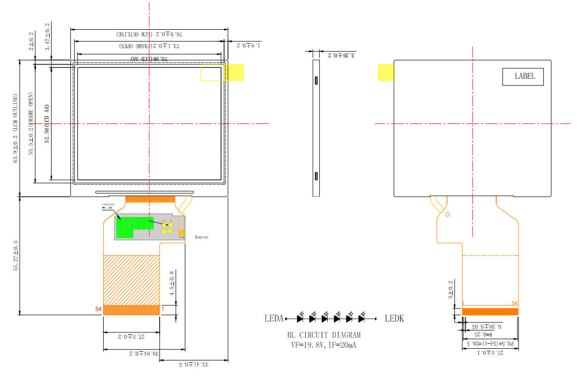


| PIN NO. | PIN NAME | DESCRIPTION |
| 1~2 | LEDK | LED backlight cathode |
| 3~4 | LEDA | LED backlight cathode |
| 5 | YU | RTP (No connection) |
| 6 | XR | RTP (No connection) |
| 7 | NC | No connection |
| 8 | RESET | Reset signal input terminal, active at ‘L’. |
| 9 | CS | Chip select signal input terminal, active at ‘L’. |
| 10 | SCK | Write signal input terminal, Active at ‘L’. Synchronizing clock signal in SPI mode. |
| 11 | SDA | SPI interface input pin |
| 12~19 | B0~B7 | Data bus |
| 20~27 | G0~G7 | Data bus |
| 28~35 | R0~R7 | Data bus |
| 36 | HSYNC | Line synchronizing signal for RGB interface operation. |
| 37 | VSYNC | Frame synchronizing signal for RGB interface operation. |
| 38 | DCLK | Dot clock signal for RGB interface operation. |
| 39~40 | NC | No connection |
| 41~42 | VCC | System power supply. |
| 43 | YD | RTP (No connection) |
| 44 | XL | RTP (No connection) |
| 45~47 | NC | No connection |
| 48~50 | IF2~IF0 | Define the input interface |
| 51 | NC | No connection |
| 52 | DE | Data ENEABLE signal for RGB interface operation. |
| 53~54 | GND | Power ground |
|
Item |
Symbol |
Min. |
Max. |
Unit |
|
Analog Supply Voltage |
VCC |
-0.3 |
4 |
V |
|
Input Voltage |
Vin |
GND-0.3 |
5 |
V |
|
Operating Temperature |
TOP |
-20 |
70 |
°C |
|
Storage Temperature |
TST |
-30 |
80 |
°C |
|
Storage Humidity |
HD |
- |
90 |
%RH |
|
Item |
Symbol |
Min. |
Typ. |
Max. |
Unit |
|
Analog Supply Voltage |
VCC |
2.5 |
- |
3.6 |
V |
|
Input High Voltage |
VIH |
0.8 |
- |
- |
V |
|
Input Low Voltage |
VIL |
0 |
- |
0.2 |
V |
|
Output High Voltage |
VOH |
0.9 |
- |
- |
V |
|
Output Low Voltage |
VOL |
0 |
- |
0.1 |
V |
|
Logic Input Current |
IIL/IIH |
-1 |
- |
1 |
uA |
|
Item |
Symbol |
MIN. |
TYP. |
MAX. |
UNIT |
Test Condition |
|
Supply Voltage |
Vf |
18.6 |
19.2 |
21 |
V |
If=20mA |
|
Supply Current |
If |
15 |
20 |
25 |
mA |
- |
|
Luminous Intensity For LCM |
- |
300 |
350 |
- |
Cd/m2 |
If=20mA |
|
Power consumption |
- |
0.279 |
0.384 |
0.525 |
W |
If=20mA |
|
Uniformity for LCM |
- |
80 |
- |
- |
% |
If=20mA |
|
Life time |
- |
30,000 |
50,000 |
- |
Hr |
- |
|
Backlight Color |
White |
|||||