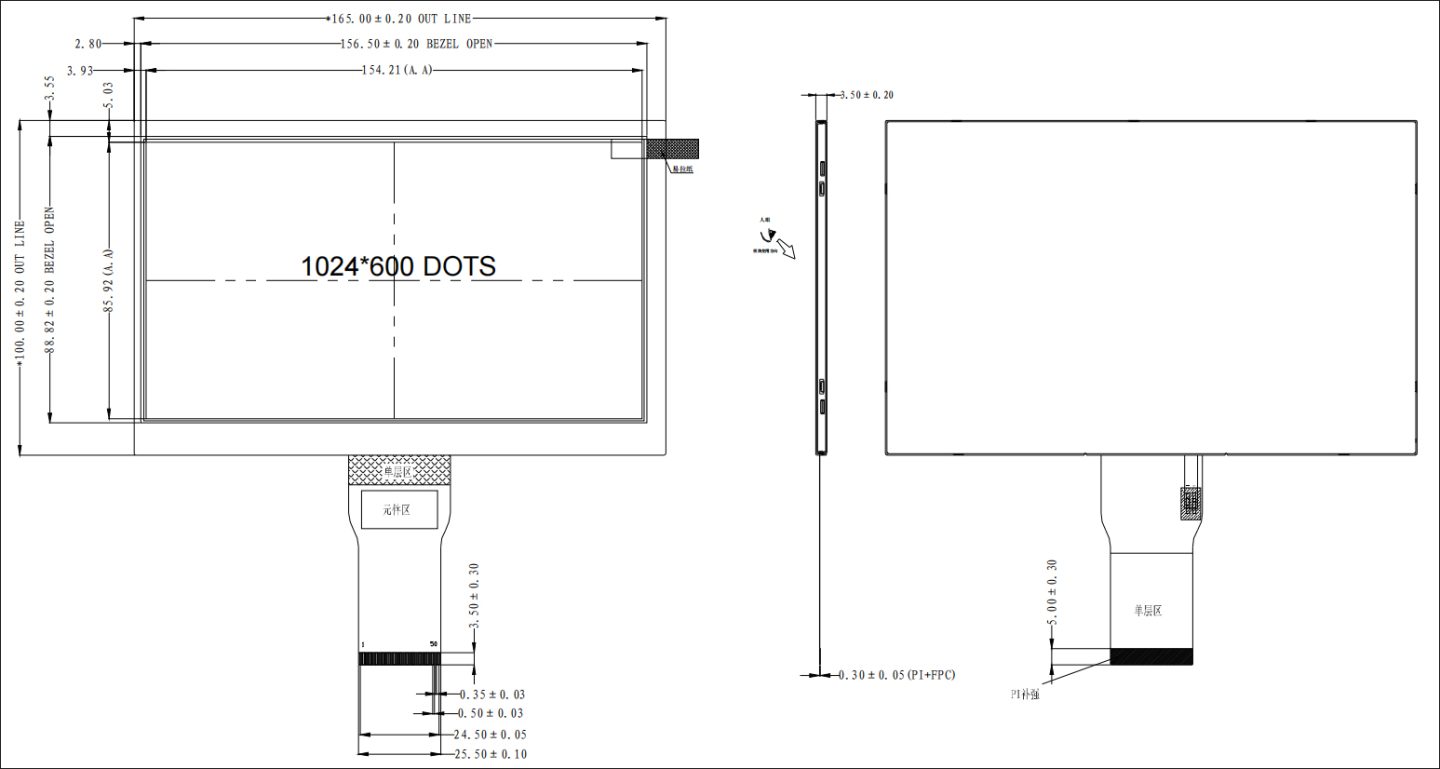


| Pin NO. | SYMBOL | I/O | DESCRIPTION |
| 1 | VLED+ | P | Power for LED backlight (Anode) |
| 2 | VLED+ | P | Power for LED backlight (Anode) |
| 3 | VLED- | P | Power for LED backlight (Cathode) |
| 4 | VLED- | P | Power for LED backlight (Cathode) |
| 5 | GND | P | Power ground |
| 6 | VCOM | I | Common Voltage |
| 7 | DVDD | P | Digital Power |
| 8 | MODE | I | DE/SYNC mode select. |
| 9 | DE | I | Data Enable signal |
| 10 | VSYNC | I | Vertical sync input |
| 11 | HSYNC | I | Horizontal sync input |
| 12~19 | B7~B0 | I | Blue data |
| 20~27 | G7~G0 | I | Green data |
| 28~35 | R7~R0 | I | Red data |
| 36 | GND | P | Power ground |
| 37 | DCLK | I | Clock input |
| 38 | GND | P | Power ground |
| 39 | SHLR | I | Left/Right Selection |
| 40 | UPDN | I | Up/Down Selection |
| 41 | VGH | P | Gate ON Voltage |
| 42 | VGL | P | Gate OFF Voltage |
| 43 | AVDD | P | Power for Analog Circuit |
| 44 | RESET | I | Global reset pin |
| 45 | NC | - | Not connection |
| 46 | VCOM | I | Common Voltage |
| 47 | DITH | I | Dithering function enable control |
| 48 | GND | P | Power ground |
| 49~50 | NC | - | Not connection |
| Item | Symbol | Min. | Max. | Unit |
| Digital Supply Voltage | VDD | -0.3 | 3.6 | V |
| Analog Supply Voltage | AVDD | -0.5 | 14.85 | V |
| TFT Gate ON Voltage | VGH | 0.3 | 20 | V |
| TFT Gate OFF Voltage | VGL | -20 | 0.3 | V |
| TFT Common Electrode Voltage | VCOM | 0 | 6 | V |
| Operating Temperature | Top | -20 | 60 | ℃ |
| Storage Temperature | Tst | -30 | 80 | ℃ |
| Item | Symbol | Min. | Typ | Max. | Unit |
| Digital Supply Voltage | VDD | 3.0 | 3.3 | 3.6 | V |
| Analog Supply Voltage | AVDD | 9 | 10 | 11 | V |
| TFT Gate ON Voltage | VGH | 18 | 19 | 20 | V |
| TFT Gate OFFVoltage | VGL | -8.5 | -7.0 | -7.5 | V |
| TFT Common Electrode Voltage | VCOM | — | 4 | — | V |
| Item | Symbol | Condition | Min | Typ | Max | Unit |
| Supply voltage | Vf | — | 9.0 | 9.6 | 10.8 | V |
| Supply current | If | — | — | 180 | — | mA |
| Number of LED | — | 3Sx9P | — | 27 | — | Pieces |