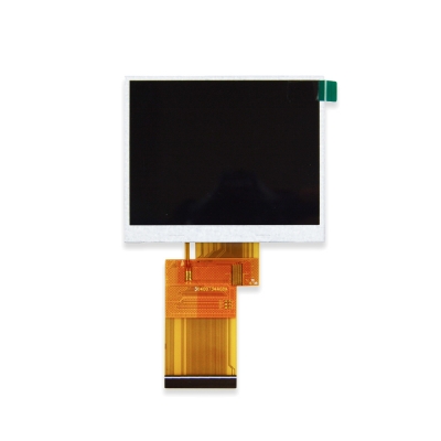
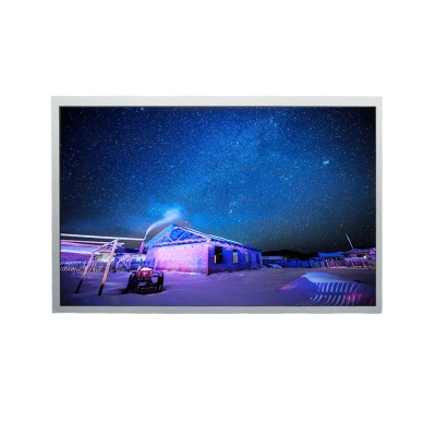
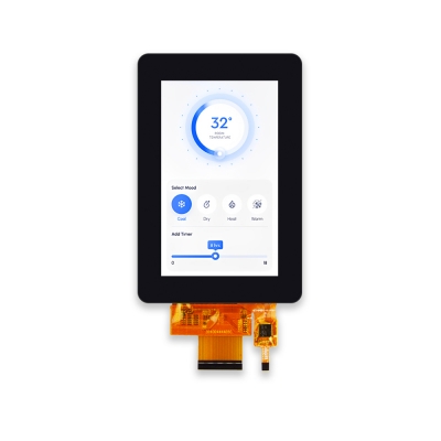
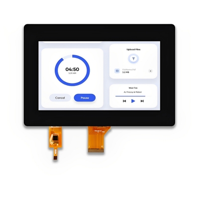
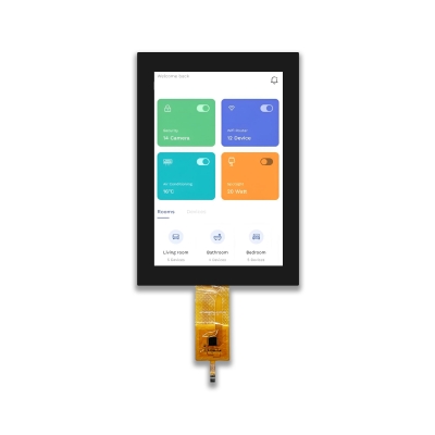
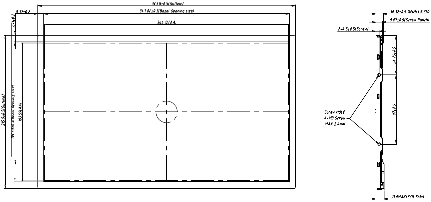
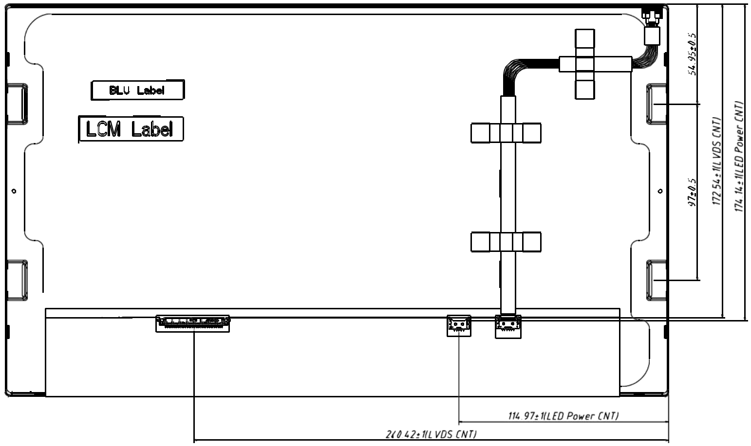
Product Structure
LCD PIN Function (LVDS 30 PIN)
|
Pin No. |
Symbol |
Description |
|
1 |
RxO0- |
Negative LVDS differential data input (Odd data) |
|
2 |
RxO0+ |
Positive LVDS differential data input (Odd data) |
|
3 |
RxO1- |
Negative LVDS differential data input (Odd data) |
|
4 |
RxO1+ |
Positive LVDS differential data input (Odd data) |
|
5 |
RxO2- |
Negative LVDS differential data input (Odd data) |
|
6 |
RxO2+ |
Positive LVDS differential data input (Odd data) |
|
7 |
GND |
Ground |
|
8 |
RxOCLK- |
Negative LVDS differential clock input (Odd clock) |
|
9 |
RxOCLK+ |
Positive LVDS differential clock input (Odd clock) |
|
10 |
RxO3- |
Negative LVDS differential data input (Odd data) |
|
11 |
RxO3+ |
Positive LVDS differential data input (Odd data) |
|
12 |
RxE0- |
Negative LVDS differential data input (Even data) |
|
13 |
RxE0+ |
Positive LVDS differential data input (Even data) |
|
14 |
GND |
Ground |
|
15 |
RxE1- |
Negative LVDS differential data input (Even data) |
|
16 |
RxE1+ |
Positive LVDS differential data input (Even data) |
|
17 |
GND |
Ground |
|
18 |
RxE2- |
Negative LVDS differential data input (Even data) |
|
19 |
RxE2+ |
Positive LVDS differential data input (Even data) |
|
20 |
RxECLK- |
Negative LVDS differential clock input (Even data) |
|
21 |
RxECLK+ |
Positive LVDS differential clock input (Even data) |
|
22 |
RxE3- |
Negative LVDS differential data input (Even data) |
|
23 |
RxE3+ |
Positive LVDS differential data input (Even data) |
|
24 |
GND |
Ground |
|
25 |
Bist |
LCD Panel Self Test Enable(3.3V Typ) |
|
26 |
SDA |
I2C-Compatible Serial-Data Input For IVO Use, Floating is recommended in the Costumer |
|
27 |
SCL |
I2C-Compatible Serial-Clock Input For IVO Use Floating is recommended in the Costumer |
|
28~30 |
VDD |
Power Supply Input Voltage (3.3V) |
|
Item |
Symbol |
Min. |
Max. |
Unit |
|
Operating Temperature |
TOP |
-30 |
85 |
℃ |
|
Storage Temperature |
TST |
-30 |
85 |
℃ |
|
Parameter |
Symbol |
Min. |
Typ. |
Max. |
Unit |
|
|
LCD Drive Voltage Logic |
VDD |
3.0 |
3.3 |
3.6 |
V |
|
|
VDD Current |
White Pattern |
IDD |
- |
- |
0.454 |
A |
|
VDD Power Consumption |
White Pattern |
PDD |
- |
- |
1.5 |
W |
|
LCD Self Test (BIST) |
High level voltage |
VBIST |
0.7*VDD |
- |
VDD |
V |
|
Low level voltage |
0 |
- |
0.3*VDD |
V |
||
|
Rush Current |
IRush |
- |
- |
1.5 |
A |
|
Backlight Characteristics
|
Parameter |
Symbol |
Min. |
Typ. |
Max. |
Unit |
|
LED Input Voltage |
VLED |
10.8 |
12.0 |
13.2 |
V |
|
LED Power Consumption |
PLED |
- |
- |
13.2 |
W |
|
LED Forward Voltage |
VF |
- |
- |
3.2 |
V |
|
LED Forward Current |
IF |
- |
70 |
|
mA |
|
White Luminance (Center) |
- |
450 |
500 |
- |
cd/m2 |
|
Luminance Uniformity (9 Points) |
- |
75 |
80 |
- |
% |
|
LED Life Time |
LT |
50,000 |
- |
- |
Hours |