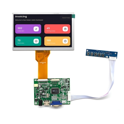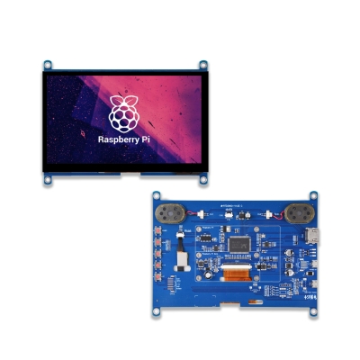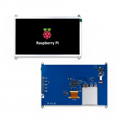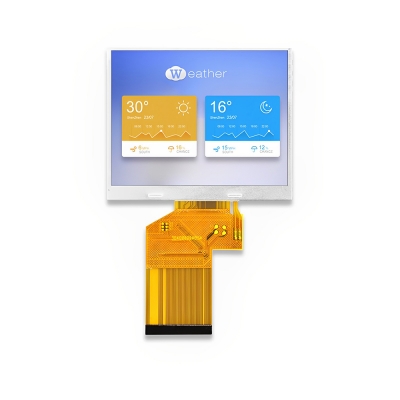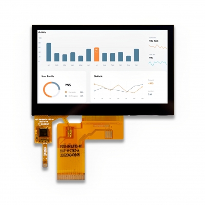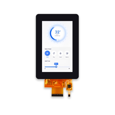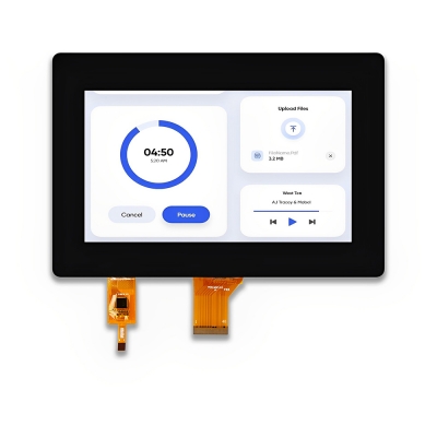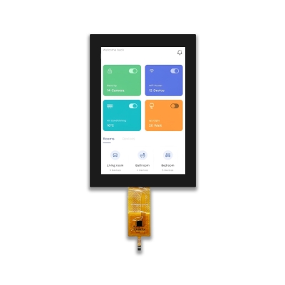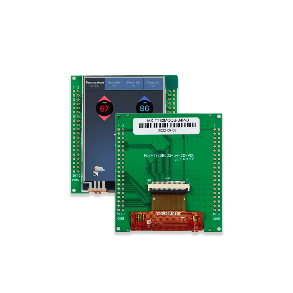


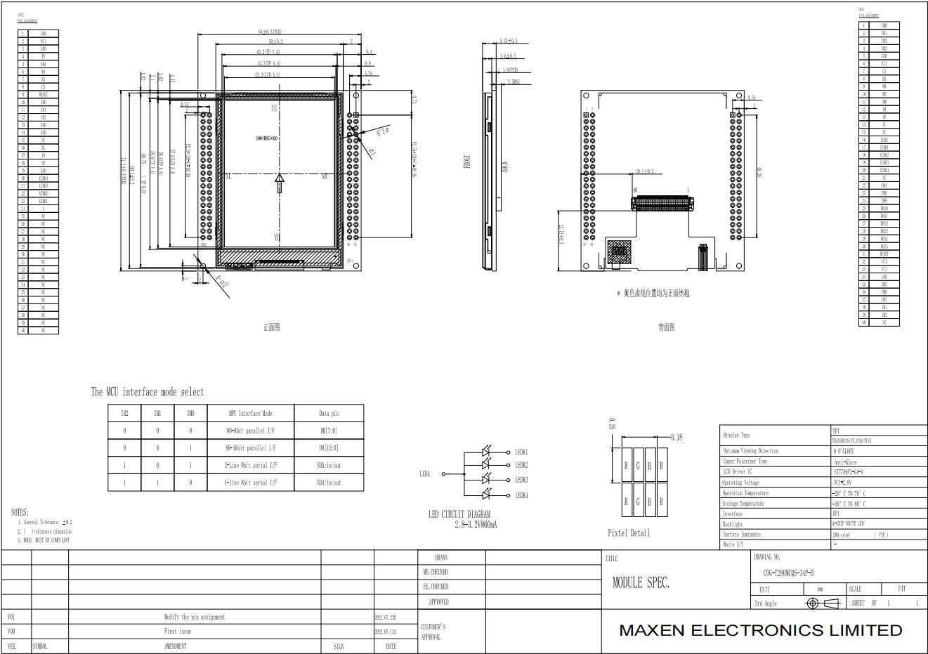
Product Structure
|
Pin No. |
Symbol |
Description |
|
1 |
DB0 |
Data bus. |
|
2 |
DB1 |
Data bus. |
|
3 |
DB2 |
Data bus. |
|
4 |
DB3 |
Data bus. |
|
5 |
GND |
Power ground |
|
6 |
VCI |
Supply voltage for analog |
|
7 |
CS |
Chip select input pin (“Low” enable). |
|
8 |
RS |
Display data/command selection pin in parallel interface. |
|
9 |
WR |
Write enable in MCU parallel interface. |
|
10 |
RD |
Read enable in 8080 MCU parallel interface. |
|
11 |
IM0 |
MCU interface mode select. |
|
12 |
XR |
Touch panel control pin |
|
13 |
YD |
Touch panel control pin |
|
14 |
XL |
Touch panel control pin |
|
15 |
YU |
Touch panel control pin |
|
16 |
LEDA |
Anode of LED backlight |
|
17 |
LEDK1 |
Cathode of LED backlight |
|
18 |
LEDK2 |
Cathode of LED backlight |
|
19 |
LEDK3 |
Cathode of LED backlight |
|
20 |
LEDK4 |
Cathode of LED backlight |
|
21 |
NC |
No connect |
|
22 |
DB4 |
Data bus. |
|
23 |
DB8 |
Data bus. |
|
24 |
DB9 |
Data bus. |
|
25 |
DB10 |
Data bus. |
|
26 |
DB11 |
Data bus. |
|
27 |
DB12 |
Data bus. |
|
28 |
DB13 |
Data bus. |
|
29 |
DB14 |
Data bus. |
|
30 |
DB15 |
Data bus. |
|
31 |
RESET |
Reset pin. Signal is active low. |
|
32 |
VCI |
Supply voltage for analog |
|
33 |
VCI |
Supply voltage for analog |
|
34 |
GND |
Power ground |
|
35 |
DB5 |
Data bus. |
|
36 |
DB6 |
Data bus. |
|
37 |
DB7 |
Data bus. |
|
38 |
IM1 |
MCU interface mode select. |
|
39 |
IM2 |
MCU interface mode select. |
|
40 |
NC |
No connect |
|
Pin No. |
Symbol |
Description |
|
1 |
GND |
Power ground |
|
2 |
VCI |
Supply voltage for analog |
|
3 |
GND |
Power ground |
|
4 |
TE |
Tearing effect signal is used to synchronize MCU to frame memory write. |
|
5 |
SDA |
Serial data input/output signal. |
|
6 |
WR |
Serial clock signal. |
|
7 |
RS |
Display data/command selection pin in parallel interface. |
|
8 |
CS |
Chip select input pin (“Low” enable). |
|
9 |
RESET |
Reset pin. Signal is active low. |
|
10 |
IM0 |
MCU interface mode select. |
|
11 |
IM1 |
|
|
12 |
IM2 |
|
|
13 |
GND |
Power ground |
|
14 |
GND |
Power ground |
|
15 |
YU |
Touch panel control pin |
|
16 |
XL |
Touch panel control pin |
|
17 |
YD |
Touch panel control pin |
|
18 |
XR |
Touch panel control pin |
|
19 |
GND |
Power ground |
|
20 |
LEDK4 |
Cathode of LED backlight |
|
21 |
LEDK3 |
Cathode of LED backlight |
|
22 |
LEDK2 |
Cathode of LED backlight |
|
23 |
LEDK1 |
Cathode of LED backlight |
|
24 |
A |
Anode of LED backlight |
|
25~40 |
NC |
No connect |
|
IM2 |
IM1 |
IM0 |
MCU interface mode |
Data pin |
|
0 |
0 |
0 |
8080-8bit parallel I/F |
DB[7:0] |
|
0 |
0 |
1 |
8080-16bit parallel I/F |
DB[15:0] |
|
1 |
0 |
1 |
3-line 9bit serial I/F |
SDA:in/out |
|
1 |
1 |
0 |
4-line 8bit serial I/F |
SDA:in/out |
|
Parameter |
Symbol |
Min |
Max |
Unit |
|
Supply voltage for analog |
VCI |
-0.3 |
4.6 |
V |
|
Supply voltage for analog |
VCI |
-0.3 |
4.6 |
V |
|
Supply current (One LED) |
ILED |
- |
30 |
mA |
|
Operating temperature |
TOP |
-20 |
70 |
°C |
|
Storage temperature |
TST |
-30 |
80 |
°C |
Electrical Characteristics
|
Item |
Symbol |
Min. |
Typ. |
Max. |
Unit |
|
Supply Voltage for Analog |
VCI |
2.4 |
2.8 |
3.3 |
V |
|
Supply Voltage for Analog |
VCI |
2.4 |
2.8 |
3.3 |
V |
|
Input Voltage |
VIL |
GND |
- |
0.3VCI |
V |
|
VIH |
07VCI |
- |
VCI |
||
|
Input leakage Current |
ILKG |
-0.1 |
- |
0.1 |
μA |
|
Item |
Symbol |
Value |
Unit |
Remark |
||
|
Min. |
Typ. |
Max. |
||||
|
Voltage for LED Backlight |
VF |
2.8 |
3 |
3.2 |
V |
IL=60mA |
|
Current for LED Backlight |
IL |
- |
60 |
- |
mA |
- |
|
Power Consumption |
P |
- |
0.18 |
- |
W |
- |
|
LED Life Time |
- |
30,000 |
50,000 |
- |
Hr |
Note |