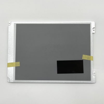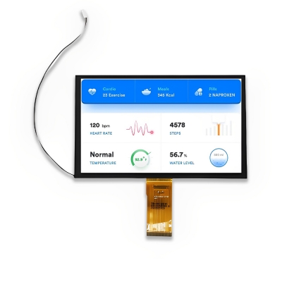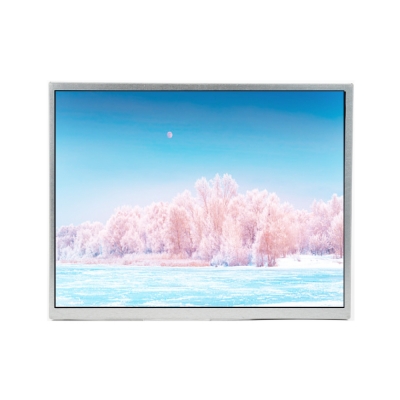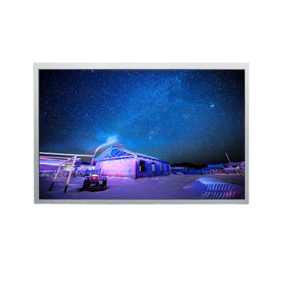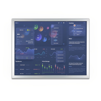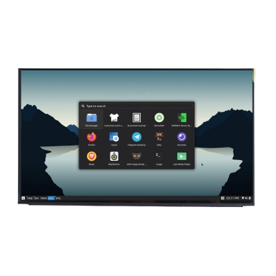


Product Structure
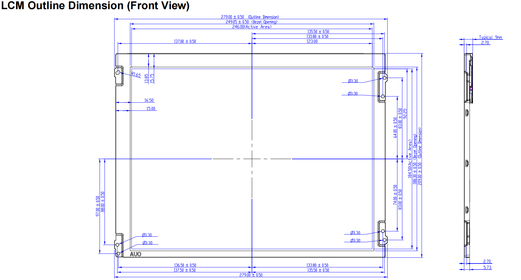
.jpg)
TFT-LCD Interface Signal Description (LVDS 20 PIN)
|
Pin No. |
Symbol |
Description |
Remark |
|
1 |
VDD |
Power Supply, 3.3V (typical) |
- |
|
2 |
VDD |
Power Supply, 3.3V (typical) |
- |
|
3 |
GND |
Ground |
- |
|
4 |
SEL68 |
6/ 8bits LVDS data input selection [H: 8bits L/NC: 6bit] |
Note1.2 |
|
5 |
RIN0- |
LVDS receiver signal channel 0 |
Note1 |
|
6 |
RIN0+ |
LVDS Differential Data Input (R0,R1,R2,R3,R4,R5,G0) |
|
|
7 |
GND |
Ground |
- |
|
8 |
RIN1- |
LVDS receiver signal channel 1 |
Note1 |
|
9 |
RIN1+ |
LVDS Differential Data Input (G1,G2,G3,G4,G5,B0,B1) |
|
|
10 |
GND |
Ground |
- |
|
11 |
RIN2- |
LVDS receiver signal channel 2 |
Note1 |
|
12 |
RIN2+ |
LVDS Differential Data Input (B2,B3,B4,B5,HS,VS,DE) |
|
|
13 |
GND |
Ground |
- |
|
14 |
CLKIN- |
LVDS receiver signal clock |
Note1 |
|
15 |
CLKIN+ |
||
|
16 |
GND |
Ground |
- |
|
17 |
RIN3- |
LVDS receiver signal channel 3 |
- |
|
18 |
RIN3+ |
LVDS Differential Data Input (R6,R7,G6,G7,B6,B7,RSV) |
Note1 |
|
19 |
REVERSE |
Reverse Scan Function [H:Enable; L/NC:Disable] |
Note1.2.3 |
|
20 |
NC/GND |
Reserved for AUO internal test. Please treat it as NC. |
Note2 |
|
Item |
Symbol |
Min. |
Max. |
Unit |
|
Logic/LCD Drive Voltage |
VDD |
-0.3 |
3.8 |
[Volt] |
|
Control Signals |
SEL68, REVERSE |
-0.3 |
VDD |
[Volt] |
|
LVDS Signals |
CLKIN-/+, RIN0~3-/+ |
-0.3 |
VDD |
[Volt] |
|
LED Input Voltage |
VCC |
-0.3 |
13 |
[Volt] |
|
LED Control Signals |
EN, PWM |
-0.3 |
6 |
[Volt] |
|
Item |
Symbol |
Min |
Max |
Unit |
|
Operating Temperature |
TOP |
-30 |
85 |
[℃] |
|
Operation Humidity |
HOP |
5 |
95 |
[%RH] |
|
Storage Temperature |
TST |
-30 |
85 |
[℃] |
|
Storage Humidity |
HST |
5 |
95 |
[%RH] |
|
Symbol |
Parameter |
Min. |
Typ. |
Max. |
Units |
Remark |
|
|
VDD |
Logic/LCD Input Voltage |
3 |
3.3 |
3.6 |
[Volt] |
- |
|
|
IVDD |
LCD Input Current |
- |
0.2 |
0.24 |
[A] |
VDD=3.3V at 60 HZ, all Black Pattern |
|
|
PVDD |
LCD Power consumption |
- |
0.66 |
0.79 |
[Watt] |
VDD=3.3V at 60 HZ, all Black Pattern |
|
|
Irush LCD |
LCD Inrush Current |
- |
- |
1.5 |
[A] |
VDD=3.3V at 60 HZ, all Black Pattern |
|
|
VDDrp |
Allowable Logic/LCD |
- |
- |
100 |
[mV] |
VDD=3.3V at 60 HZ, all Black Pattern |
|
|
VIH |
Control Signals |
High Level |
0.7*VDD |
- |
VDD |
[Volt] |
SEL68 and REVERSE |
|
VIL |
Low Level |
0 |
- |
0.3*VDD |
[Volt] |
SEL68 and REVERSE |
|
|
Symbol |
Parameter |
Min. |
Typ. |
Max. |
Unit |
Remark |
|
|
VCC |
Input Voltage |
10.8 |
12 |
12.6 |
[Volt] |
- |
|
|
IVCC |
Input Current |
- |
0.33 |
0.4 |
[A] |
VCC=12V & 100% |
|
|
PVCC |
Power Consumption |
- |
3.96 |
4.8 |
[Watt] |
VCC=12V & 100% |
|
|
VEN |
EN Control Level |
BL On |
3 |
- |
5.5 |
[Volt] |
- |
|
BL Off |
0 |
- |
0.5 |
[Volt] |
- |
||
|
FPWM |
Dimming Frequency |
200 |
- |
20K |
[Hz] |
- |
|
|
DPWM |
Dimming Duty Cycle |
5 |
- |
100 |
% |
- |
|
|
VPWM |
Dimming Control Level |
High Level |
3 |
- |
5.5 |
[Volt] |
- |
|
Low Level |
0 |
- |
0.5 |
[Volt] |
|||
|
IF |
LED Forward Current |
- |
45 |
|
[mA] |
Ta=25℃ |
|
|
VF |
LED Forward Voltage |
- |
3.2 |
3.6 |
[Volt] |
IF=45mA,Ta=25℃ |
|
|
PLED |
LED Power Consumption |
- |
3.02 |
3.4 |
[Watt] |
- |
|
|
- |
LED life time |
50,000 |
- |
- |
Hrs |
IF=45mA,Ta=25℃ |
|