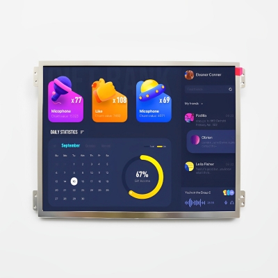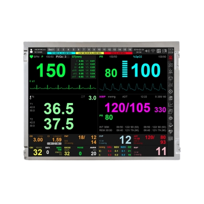


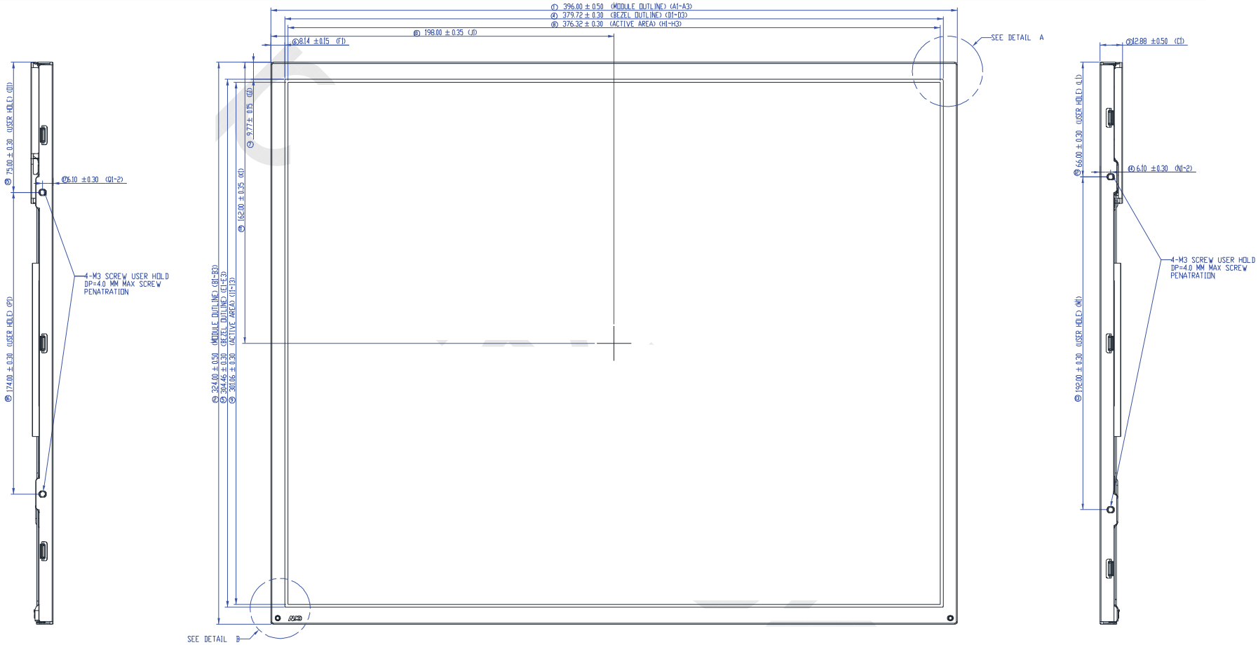
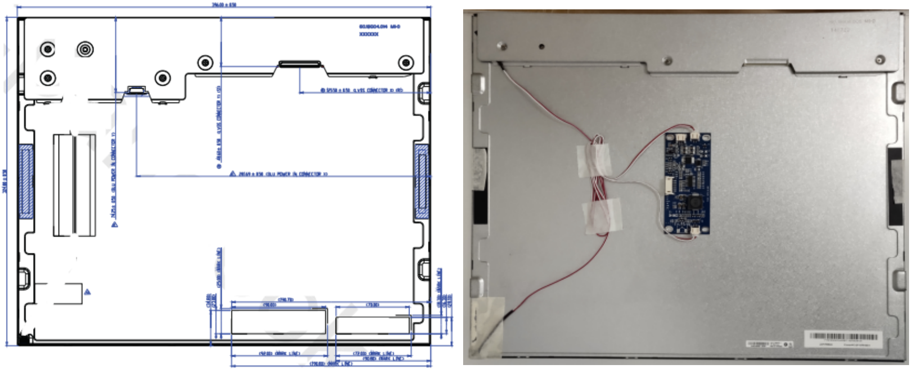
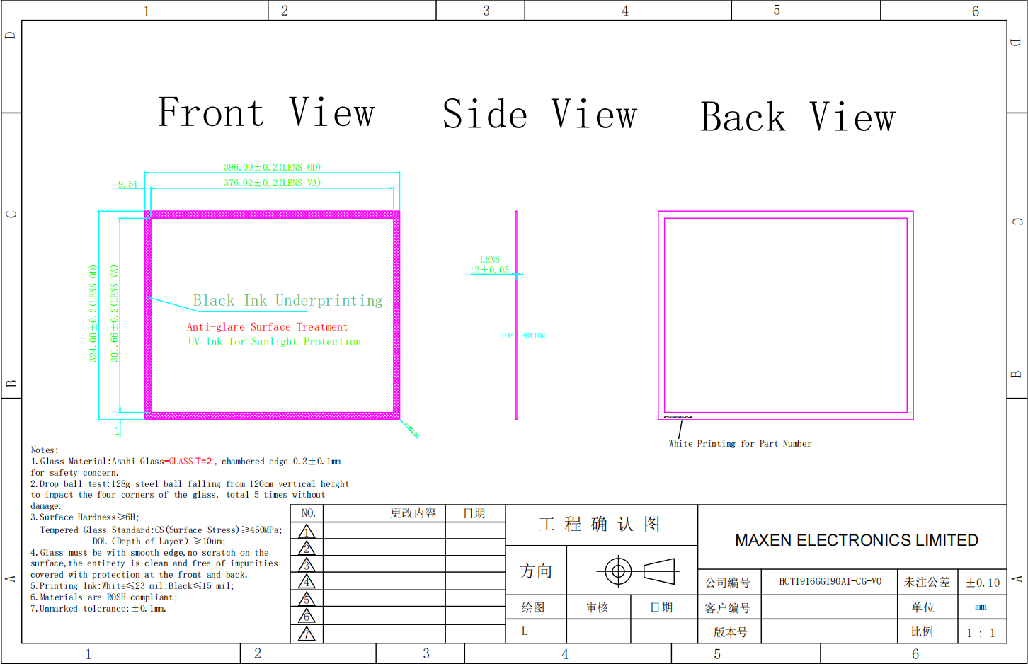
Product Structure
LCD PIN Function (LVDS 30 PIN)
|
PIN # |
Signal Name |
Description |
|
1 |
RxOIN0- |
Negative LVDS differential data input (Odd data) |
|
2 |
RxOIN0+ |
Positive LVDS differential data input (Odd data) |
|
3 |
RxOIN1- |
Negative LVDS differential data input (Odd data) |
|
4 |
RxOIN1+ |
Positive LVDS differential data input (Odd data) |
|
5 |
RxOIN2- |
Negative LVDS differential data input (Odd data, DSPTMG) |
|
6 |
RxOIN2+ |
Positive LVDS differential data input (Odd data, DSPTMG) |
|
7 |
GND |
Power Ground |
|
8 |
RxOCLKIN- |
Negative LVDS differential clock input (Odd clock) |
|
9 |
RxOCLKIN+ |
Positive LVDS differential clock input (Odd clock) |
|
10 |
RxOIN3- |
Negative LVDS differential data input (Odd data) |
|
11 |
RxOIN3+ |
Positive LVDS differential data input (Odd data) |
|
12 |
RxEIN0- |
Negative LVDS differential data input (Even data) |
|
13 |
RxEIN0+ |
Positive LVDS differential data input (Even data) |
|
14 |
GND |
Power Ground |
|
15 |
RxEIN1- |
Negative LVDS differential data input (Even data) |
|
16 |
RxEIN1+ |
Positive LVDS differential data input (Even data) |
|
17 |
GND |
Power Ground |
|
18 |
RxEIN2- |
Negative LVDS differential data input (Even data) |
|
19 |
RxEIN2+ |
Positive LVDS differential data input (Even data) |
|
20 |
RxECLKIN- |
Negative LVDS differential data input (Even clock) |
|
21 |
RxECLKIN+ |
Positive LVDS differential data input (Even clock) |
|
22 |
RxEIN3- |
Negative LVDS differential data input (Even data) |
|
23 |
RxEIN3+ |
Positive LVDS differential data input (Even data) |
|
24~27 |
GND |
Power Ground |
|
28~30 |
POWER |
Power +5V |
|
Item |
Symbol |
Min. |
Max. |
Unit |
|
Operating Temperature |
TOP |
-30 |
85 |
℃ |
|
Storage Temperature |
TST |
-30 |
85 |
℃ |
|
Parameter |
Symbol |
Min. |
Typ. |
Max. |
Unit |
|
Logic/LCD Driver Voltage |
VDD |
4.5 |
5.0 |
5.5 |
V |
|
Input Current |
IDD |
- |
1 |
1.2 |
A |
|
VDD Power |
PDD |
- |
5 |
6 |
W |
|
Inrush Current |
IRush |
- |
- |
3.0 |
A |
|
Allowable Logic/LCD Drive Ripple Voltage |
VDDrp |
- |
- |
100 |
mV |
|
Parameter |
Symbol |
Min. |
Typ. |
Max. |
Unit |
|
LED Forward Current |
IF |
- |
100 |
- |
mA |
|
LED Forward Voltage |
VF |
33.6 |
38.4 |
43.2 |
V |
|
LED Power Consumption |
PLED |
- |
- |
20 |
W |
|
Central Luminance |
- |
950 |
1000 |
- |
cd/m2 |
|
Luminance Uniformity |
- |
75 |
80 |
- |
% |
|
LED Life Time |
- |
- |
50000 |
- |
Hrs |