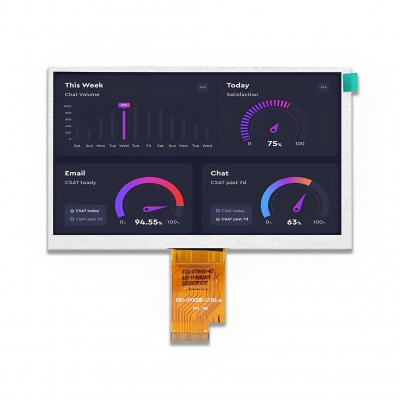

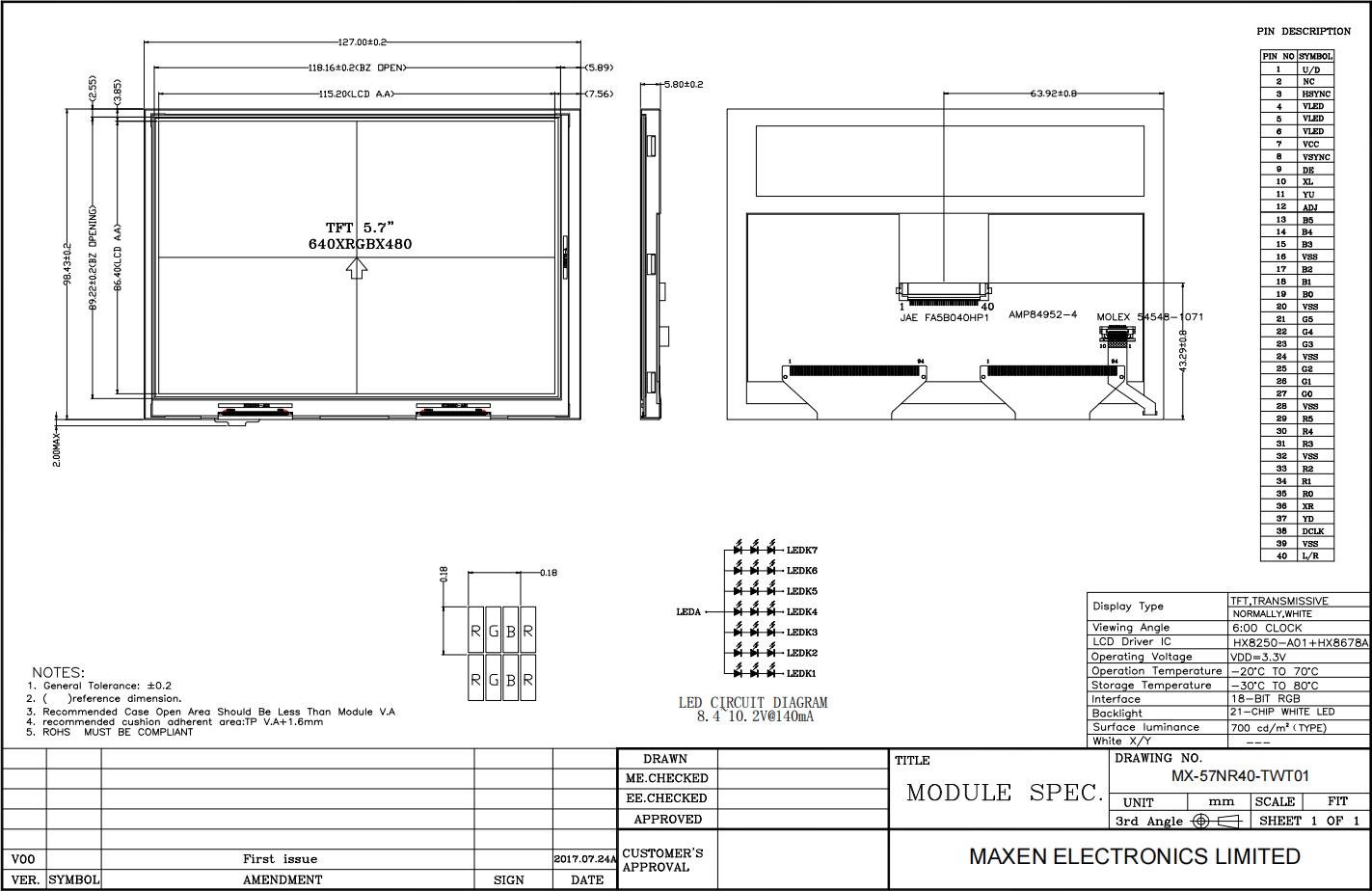
LCD PIN Function
|
Pin No. |
Symbol |
Description |
|
1 |
U/D |
Up/down scan setting. When U/D=H, reverse scan. When U/D=L, normal scan. |
|
2 |
NC |
No connection. |
|
3 |
HSYNC |
Horizontal sync input in digital RGB and CCIR601 mode. (Short to GND if not used) |
|
4~6 |
VLED |
Power supply for BLU LDO circuit. |
|
7 |
VCC |
Power supply. |
|
8 |
VSYNC |
Vertical sync input in digital RGB and CCIR601 mode. (Short to GND if not used) |
|
9 |
DE |
Input data enable control. When DE mode, active High to enable data input. Default pull low. |
|
10 |
NC(X2) |
No connection. (Touch panel control PIN:X2) |
|
11 |
NC(Y1) |
No connection. (Touch panel control PIN:Y1) |
|
12 |
ADJ |
Chip Enable (Active High). |
|
13~15 |
B5~B3 |
Blue data input. |
|
16 |
VSS |
Power ground. |
|
17~19 |
B2~B0 |
Blue data input. |
|
20 |
VSS |
Power ground. |
|
21~23 |
G5~G3 |
Green data input. |
|
24 |
VSS |
Power ground. |
|
25~27 |
G2~G0 |
Green data input. |
|
28 |
VSS |
Power ground. |
|
29~31 |
R5~R3 |
Red data input. |
|
32 |
VSS |
Power ground. |
|
33~35 |
R2~R0 |
Red data input. |
|
36 |
NC(X1) |
No connection. (Touch panel control PIN:X1) |
|
37 |
NC(Y2) |
No connection. (Touch panel control PIN:Y2) |
|
38 |
DCLK |
Clock signal. Latching data at the rising edge. |
|
39 |
VSS |
Power ground. |
|
40 |
L/R |
The shift direction of device internal shift register is controlled by this pin as shown below: L/R=H: STH->SO1->• • •->SO960->STHO L/R=L: STH->SO960->• • •->SO1->STHO |
Absolute Maximum Ratings
|
Parameter |
Symbol |
Min. |
Max. |
Unit |
|
Supply voltage for analog |
VCC |
-0.5 |
5 |
V |
|
Supply voltage for logic |
VCC |
-0.5 |
5 |
V |
|
Supply current (One LED) |
ILED |
|
40 |
mA |
|
Operating temperature |
TOP |
-20 |
70 |
℃ |
|
Storage temperature |
TST |
-30 |
80 |
℃ |
Electrical Characteristics
|
Item |
Symbol |
Min. |
Typ. |
Max. |
Unit |
Applicable terminal |
|
Supply Voltage for Analog |
VCC |
2.7 |
3.3 |
3.6 |
V |
|
|
Supply Voltage for Logic |
VCC |
2.7 |
3.3 |
3.6 |
V |
|
|
Input Voltage |
VIL |
-0.3 |
- |
0.2VCC |
V |
|
|
VIH |
0.8VCC |
- |
VCC |
|||
|
Input leakage Current |
ILKG |
-1 |
|
1 |
μA |
|
Backlight Characteristics
|
Item |
Symbol |
Value |
Unit |
Remark |
||
|
Min. |
Typ. |
Max. |
||||
|
Voltage for LED Backlight |
VF |
8.4 |
9.6 |
10.2 |
V |
IL=140mA |
|
Current for LED Backlight |
IL |
|
140 |
|
mA |
|
|
Power Consumption |
P |
|
1.344 |
|
W |
|
|
LED Life Time |
|
30,000 |
50,000 |
|
Hr |
Note |
|
Power supply for LED |
VLED |
4.5 |
5 |
5.5 |
V |
|
|
ADJ frequency |
|
19K |
20K |
21K |
Hz |
|
|
ADJ input voltage |
VIH |
3 |
|
3.3 |
V |
|
|
ADJ input voltage |
VIL |
0 |
|
0.3 |
V |
|