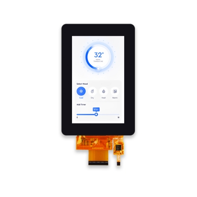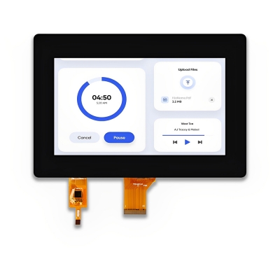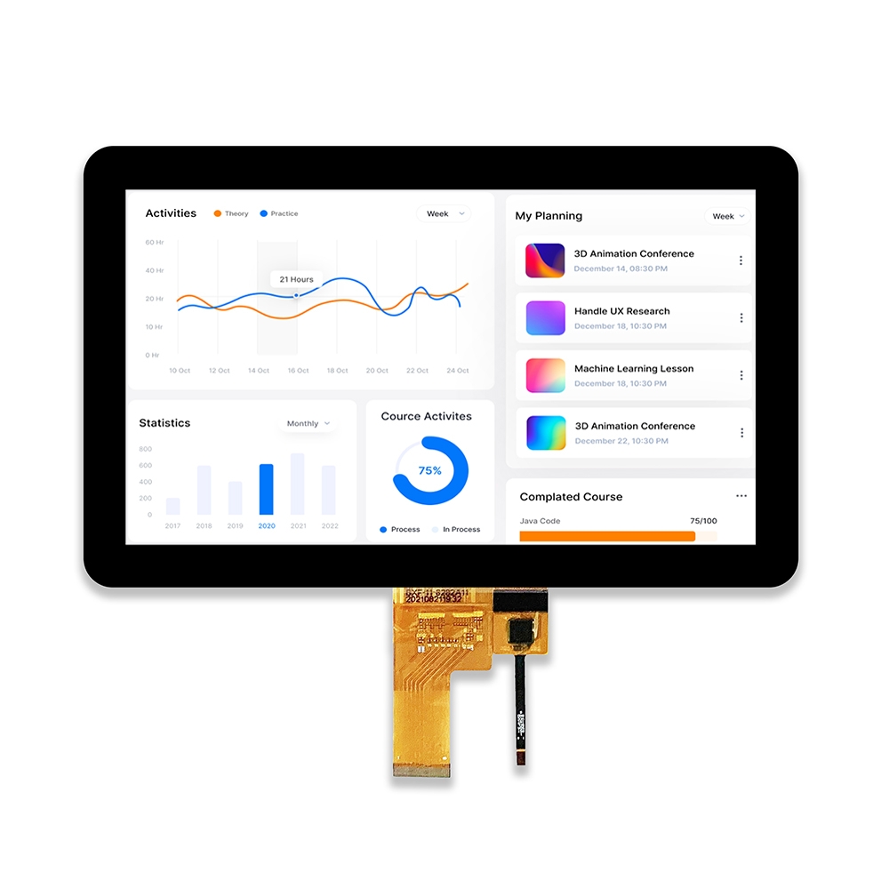

Product Structure
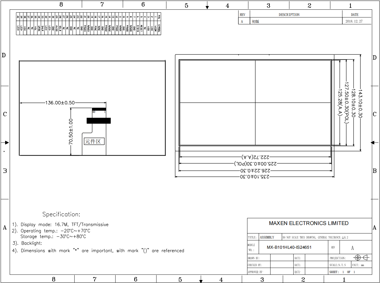
|
Pin NO. |
Symbol |
Description |
|
1 |
VCOM |
Common voltage |
|
2~3 |
VDD |
Digital Power |
|
4 |
NC |
No connection |
|
5 |
Reset |
Global reset pin. Active Low to enter Reset State. Normally pull high. It’s necessary to connecting with an RC delay circuit for stability. (GRB delay VDD larger than 1ms) |
|
6 |
STBYB |
Standby mode, normally pull high STBYB=”1”, Normal Operation STBYB=”0”, Timing control, source driver will turn off, all output are high-Z |
|
7 |
GND |
Ground level for analog block. |
|
8 |
NIND0 |
Negative LVDS Differential Data Inputs |
|
9 |
PIND0 |
Positive LVDS Differential Data Inputs |
|
10 |
GND |
Ground |
|
11 |
NIND1 |
Negative LVDS Differential Data Inputs |
|
12 |
PIND1 |
Positive LVDS Differential Data Inputs |
|
13 |
GND |
Ground |
|
14 |
NIND2 |
Negative LVDS Differential Data Inputs |
|
15 |
PIND2 |
Positive LVDS Differential Data Inputs |
|
16 |
GND |
Ground |
|
17 |
NINC |
Negative LVDS Differential Clock Inputs |
|
18 |
PINC |
Positive LVDS Differential Clock Inputs |
|
19 |
GND |
Ground |
|
20 |
NIND3 |
Negative LVDS Differential Data Inputs |
|
21 |
PIND3 |
Positive LVDS Differential Data Inputs |
|
22 |
GND |
Ground |
|
23~24 |
NC |
No connection |
|
25 |
GND |
Ground |
|
26~27 |
NC |
No connection |
|
28 |
SELB |
6bit / 8bit mode select |
|
29 |
AVDD |
Power for Analog Circuit |
|
30 |
GND |
Ground |
|
31~32 |
LED- |
LED Cathode |
|
33 |
SHLR |
Horizontal Inversion |
|
34 |
UPDN |
Vertical Inversion |
|
35 |
VGL |
Negative Power for TFT. |
|
36~37 |
NC |
No connection |
|
38 |
VGH |
Positive Power for TFT. |
|
39~40 |
LED+ |
LED Anode |
|
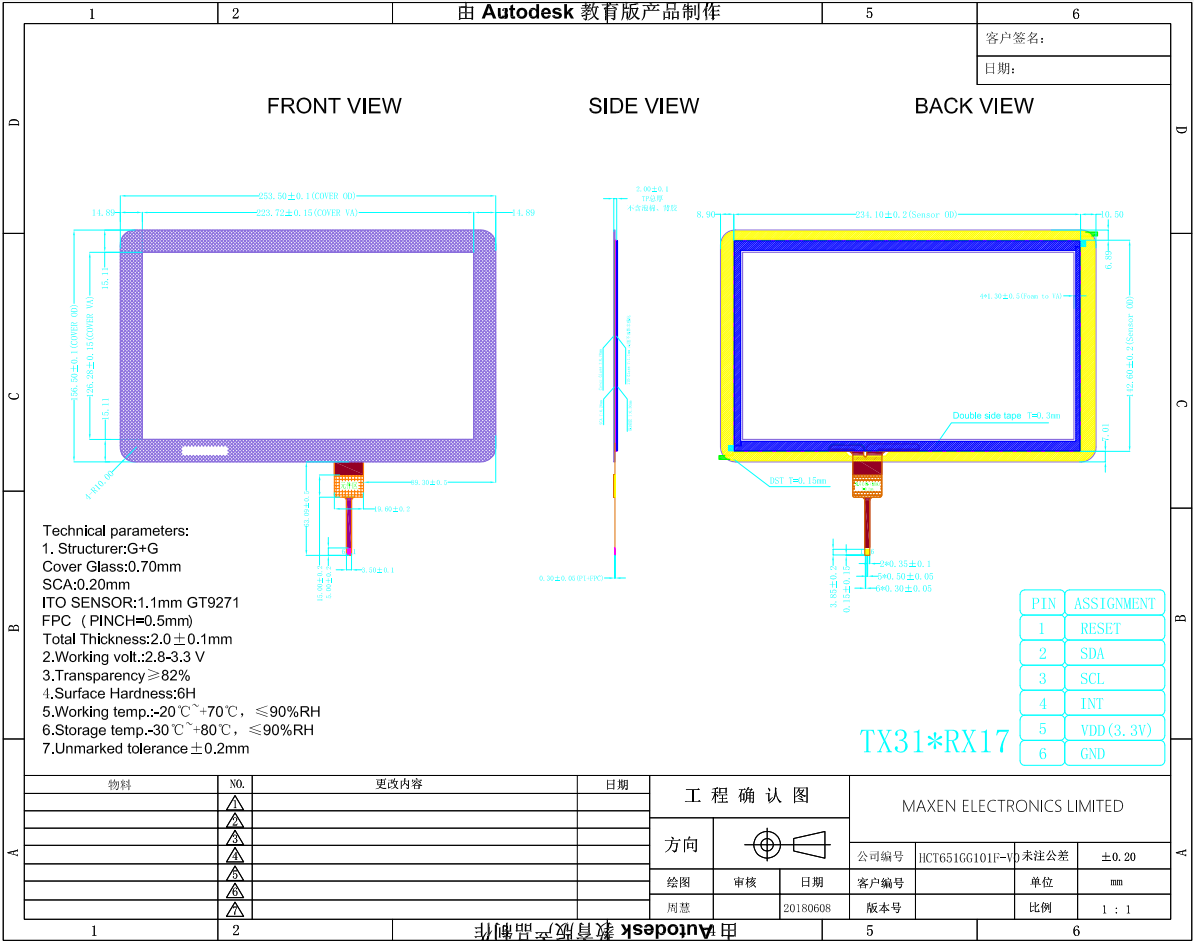
PIN NO. |
ASSIGNMENT |
|
1 |
RESET |
|
2 |
SDA |
|
3 |
SCL |
|
4 |
INT |
|
5 |
VDD (3.3V) |
|
6 |
GND |