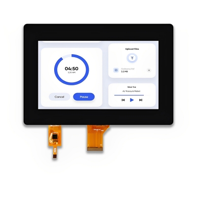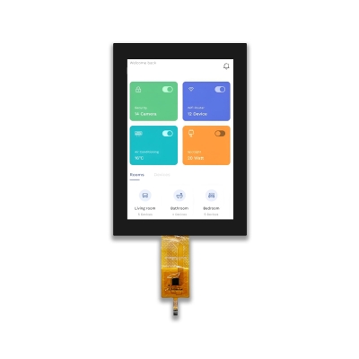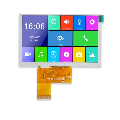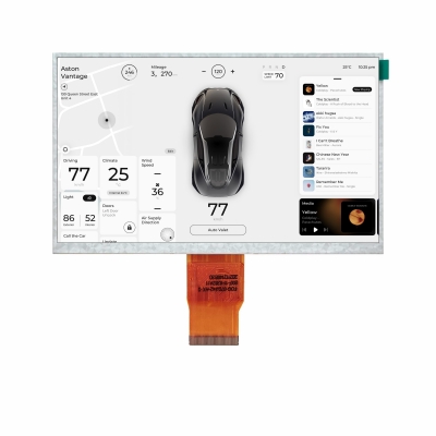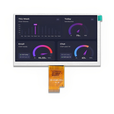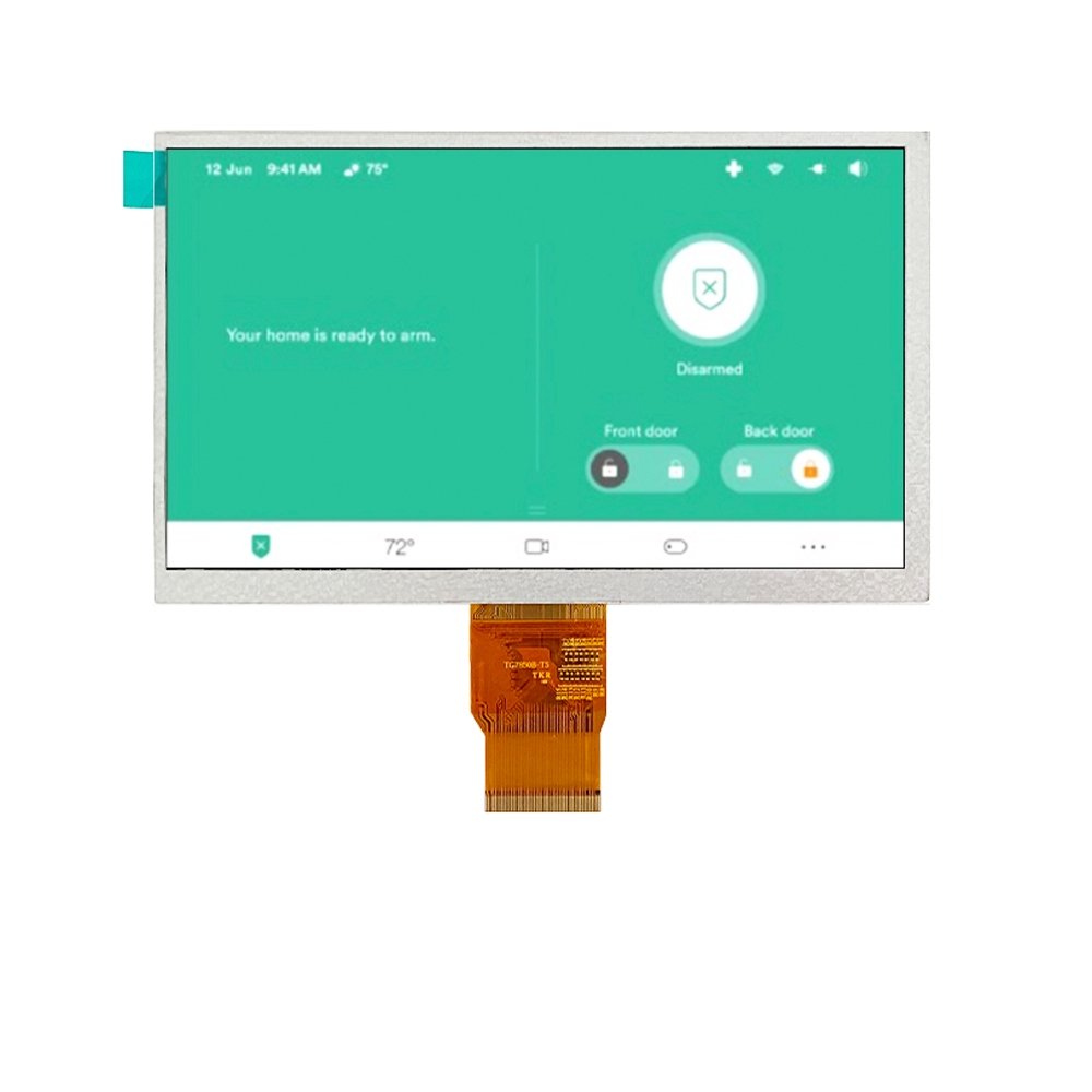


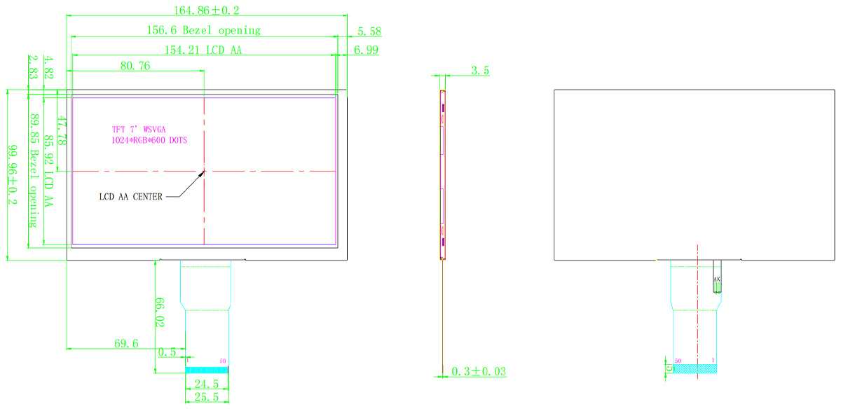
Product Structure
|
Pin No. |
Symbol |
Functional |
|
1 |
LEDA |
LED Anode |
|
2 |
LEDA |
LED Anode |
|
3 |
LEDK |
LED Cathode |
|
4 |
LEDK |
LED Cathode |
|
5 |
GND |
Digital Ground |
|
6 |
VCOM |
For external VCOM DC input |
|
7 |
DVDD |
Digital Power |
|
8 |
MODE |
DE/SYNC mode select |
|
9 |
DE |
Data enable signal |
|
10 |
VSYNC |
Vertical sync input |
|
11 |
HSYNC |
Horizontal sync input |
|
12~19 |
B7~B0 |
Blue data Input |
|
20~27 |
G7~G0 |
Green data Input |
|
28~35 |
R7~R0 |
Red data Input |
|
36 |
GND |
Digital Ground |
|
37 |
DCLK |
Clock input |
|
38 |
GND |
Digital Ground |
|
39 |
L/R |
Source right or left sequence control |
|
40 |
U/D |
Gate up or down scan control |
|
41 |
VGH |
Positive Power for TFT |
|
42 |
VGL |
Negative Power for TFT |
|
43 |
AVDD |
Analog Power |
|
44 |
RSTB |
Global reset pin.Active low to enter reset state |
|
45 |
NC |
Not connect |
|
46 |
VCOM |
For external VCOM DC input |
|
47 |
DITHB |
Dithering setting |
|
48 |
GND |
Digital Ground |
|
49 |
NC |
Not connect |
|
50 |
NC |
Not connect |
|
Parameter |
Symbol |
Min |
Max |
Unit |
|
Power supply 1 |
VDD |
-0.5 |
3.96 |
V |
|
Power supply 2 |
Avdd |
-0.5 |
13.85 |
V |
|
Operating temperature |
TOPR |
-20 |
70 |
℃ |
|
Storage temperature |
TSTG |
-30 |
80 |
℃ |
|
VDD |
3.3V |
|
AVDD |
9.6V |
|
VCOM |
3.8V |
|
VGH |
18V |
|
VGL |
-6V |
|
Item |
Symbol |
Min. |
Typ. |
Max. |
Unit |
|
LED module Forward voltage |
VLED |
- |
9.3 |
9.6 |
V |
|
LED module current |
ILED |
- |
120 |
- |
mA |
|
L/G Surface Luminance★1 |
LS |
- |
280 |
- |
Mc/d2 |
|
LCM Surface brightness uniform★2 |
LD |
80 |
- |
- |
% |
|
LED Life Time |
- |
30,000 |
50,000 |
- |
Hr |