





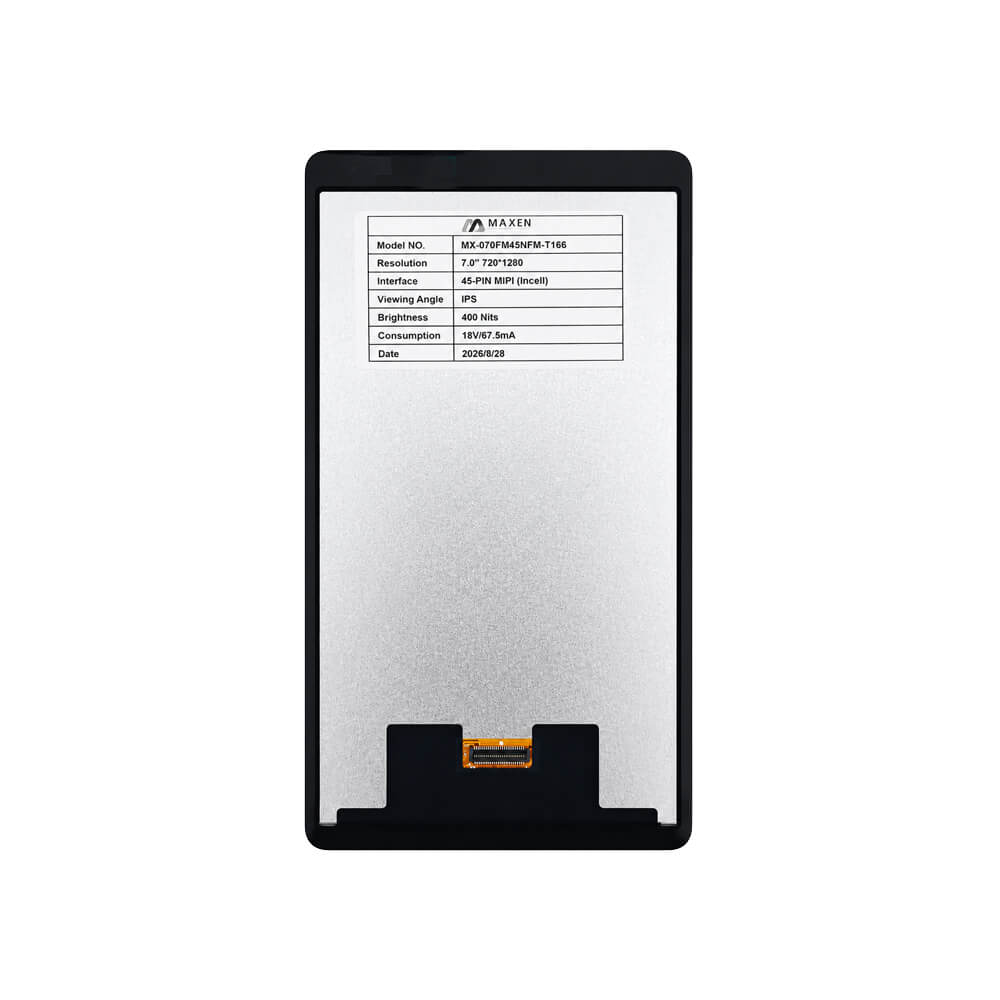



LCM Pin Definition (45-pin MIPI)
| PIN NO. | Symbol | Description |
| 1 | GND | Ground |
| 2 | GND | Ground |
| 3 | AVDD | 5.8V input power |
| 4 | AVDD | 5.8V input power |
| 5 | NC | NC |
| 6 | AVEE | -5.8V input power |
| 7 | AVEE | -5.8V input power |
| 8 | GND | Ground |
| 9 | GND | Ground |
| 10 | D3- | MIPI differential data3 input(Negative) |
| 11 | D3+ | MIPI differential data3 input(Positive) |
| 12 | GND | Ground |
| 13 | D0- | MIPI differential data0 input(Negative) |
| 14 | D0+ | MIPI differential data0 input(Positive) |
| 15 | GND | Ground |
| 16 | CLK- | MIPI differential clock input(Negative) |
| 17 | CLK+ | MIPI differential clock input(Positive) |
| 18 | GND | Ground |
| 19 | D1- | MIPI differential datal input(Negative) |
| 20 | D1+ | MIPI differential datal input(Positive) |
| 21 | GND | Ground |
| 22 | D2- | MIPI differential data2 input(Negative) |
| 23 | D2+ | MIPI differential data2 input(Positive) |
| 24 | GND | Ground |
| 25 | GND | Ground |
| 26 | ID0 | System Hardware IDO Select |
| 27 | ID1 | System Hardware ID1 Select |
| 28 | LEDPWM_OUT | Output pin for PWM signal of LED driving |
| 29 | TE | TE |
| 30 | REST | This signal will reset the device and must be Applied properly to initialize the chip |
| 31 | VDD18 | Power supply 1.8V |
| 32 | VDD18 | Power supply 1.8V |
| 33 | GND | Ground |
| 34 | TP-SCL | I2C CLK,TYP.1.8V |
| 35 | TP-SDA | I2C SDA,TYP.1.8V |
| 36 | TP-INT | Interrupt signal for TP |
| 37 | TP-RST | The extemal reset input for TP |
| 38 | GND | Ground |
| 39 | FB1 | Power for LED1 Cathode |
| 40 | FB2 | Power for LED2 Cathode |
| 41 | FB3 | Power for LED3 Cathode |
| 42 | FB4 | Power for LED4 Cathode |
| 43 | NC | NC |
| 44 | VLED | Power for LED Anode |
| 45 | VLED | Power for LED Anode |